Chapter 2 Function Generator Operation
©
National Instruments Corporation 2-11 NI 5401 User Manual
Pre-Attenuation Offset
The NI 5401 hardware supports a DC offset of up to ±2.5 V before the
attenuation chain. Unless the 10 dB attenuator is switched in, which occurs
when the amplitude is less then 3.16 V
pk-pk
, the waveform maximum plus
the offset must not exceed ±5 V into 50 Ω. If it does, the waveform is
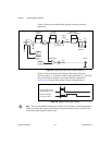
clipped. Refer to Figure 2-8 for a diagram showing the location of the
10 dB attenuator.
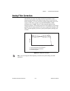
NI-FGEN automatically calculates the pre-attenuation offset value based
on the DC offset and amplitude values, so the allowable DC offset range is
dependent on the amplitude. For example, if you have an amplitude of
1V
pk-pk
, the maximum DC offset you can apply is 0.25 V, which
corresponds to a pre-attenuation offset of 2.5 V.
Note
You can change the DC Offset at any time during waveform generation. Refer to
your software documentation for additional information.
Phase-Locked Loops and Board Synchronization
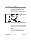
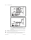
Figure 2-11 illustrates the block diagram for the NI 5401 for PCI PLL
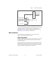
circuit. Figure 2-12 illustrates the block diagram for the NI 5401 for PXI
PLL circuit. The PLL consists of a voltage-controlled crystal oscillator
(VCXO) with a tuning range of ±100 ppm. This VCXO generates the main
clock of 80 MHz.
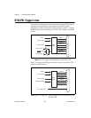
The PLL can lock to a reference clock source from the external connector,
from a RTSI Osc line on the RTSI bus (NI 5401 for PCI), or from a
10 MHz Osc line on the PXI backplane bus (for NI 5401 for PXI). The PLL
can also be tuned internally using a calibration DAC (CalDAC). National
Instruments accurately performs this tuning during manufacturing. Refer to
the RTSI/PXI Trigger Lines section later in this manual for additional
information on using the RTSI and 10 MHz Osc lines.
The reference and VCXO clock are compared by a phase comparator
running at 1 MHz. The loop filters the error signal and sends it to the control
pin of the VCXO to complete the loop.


