Chapter 2 Function Generator Operation
NI 5401 User Manual 2-12 www.natinst.com
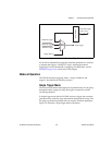
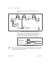
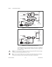
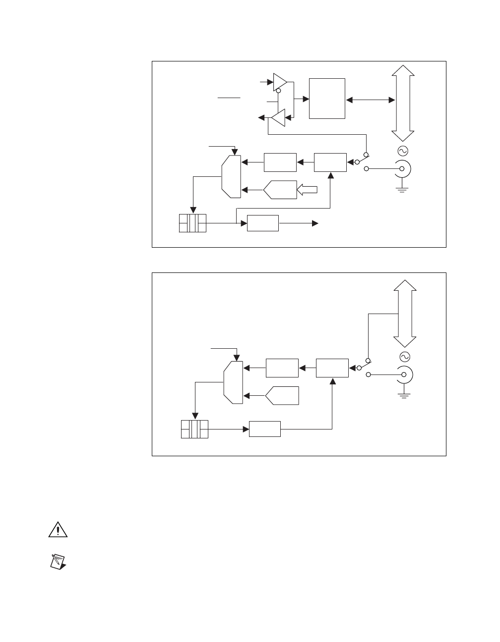
Figure 2-11. PLL Architecture for the NI 5401 for PCI
Figure 2-12. PLL Architecture for the NI 5401 for PXI
You can frequency lock to an external reference clock source of 1 MHz and
from 5–20 MHz in 1 MHz increments. The PLL can lock to a signal level
of at least 1 V
pk-pk
.
Caution Do not increase the voltage level of the clock signal at the PLL reference input
connector by more than the specified limit, 5 V
pk-pk
.
Note If two or more NI 5401 devices are locked to each other using the same reference
clock, they are frequency locked, but the phase relationship is indeterminate.
80 MHz
Div/4
VCXO
Board Clock (Master)
RTSI Clock (Slave)
Master/Slave
RTSI
Switch
RTSI Bus
RTSI Osc
Board Clock
20 MHz
Loop
Filter
Tune
DAC
PLL Ref
(1 V
pk-pk
min)
Control
Voltage
(20 MHz)
Source
14
Phase
Comp
AMUX
80 MHz
Div/8
VCXO
PXI Bus
10 MHz
Loop
Filter
CAL
DAC
PLL Ref
(1 V
pk-pk
min)
Control
Voltage
10 MHz Osc
Source
Phase
Comp
AMUX


