


CHAPTER 4 CAUTIONS
User’s Manual U15776EJ1V0UM
29
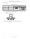
(3) The V
DD1
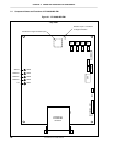
signal from the target system is left open in the IE-703089-MC-EM1.
(4) The following conditions must be satisfied when other than V
DD0
= V
DD1
= ADCV
DD
= PORTV
DD1
= PORTV
DD2
.
1. When FCAN is used, PORTV
DD1
≤ PORTV
DD2
(restricted by the power supply voltage conditions of the in-
circuit emulator)
2. When ADC is used, V
DD0
= ADCV
DD
= 4.5 to 5.5 V
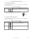
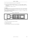
4.2 I/O Signal
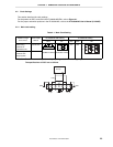
The input signal (NMI signal) from the target system, the I/O signals for ports 4, 5, 6, and 11, and the I/O signal for
port 9 are all delayed (t
PD
= 0.25 ns (typ.)) because they pass through Q switches QS3125, QS3384, and QS3244,
respectively, before being input to the emulator chip.
The DC characteristics also change. The input voltage becomes V
IH
= 2.0 V (MIN.), V
IL
= 0.8 V (MAX.), and the
input current becomes I
IN
= ±0.5
µ
A (MAX.).
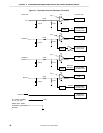
Figure 4-2. I/O Signal Flow Path
NMI pin QS3125
IE-703089-MC-EM1
Port pin
QS3384/
QS3244
Target
system
Emulator chip
NMI signal
Port signal
4.3 V
PP
Signal
The V
PP
signal from the target system is left open in the emulator.
4.4 NMI Signal Mask Function
When using the P00/NMI pin in the port mode, do not mask the NMI signal.