


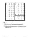
DDR3THIN-MN-XXX 38 Doc. Rev. 1.11
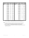
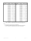
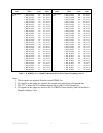
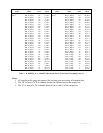
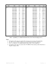
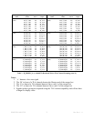
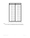
Group
Name
Signal
Name
DDR3
Pin #
TLA
Input
Group
Name
Signal
Name
DDR3
Pin #
TLA
Input
Control
2
CKE1 169 M_A3:2 Address
2
BA2 52 M_A3:0
(SYM) CKE0 50 M_A3:1 (Hex) BA1 190 M_C3:7
S3# 49 S2_C2:5 BA0 71 M_C1:6
S2# 48 S2_C3:0 A15 171 M_CK0
S1# 76 M_C3:4 A14 172 M_A2:5
S0# 193 M_C3:3 A13 196 M_CK3
BA2 52 M_A3:0 A12/BC# 174 M_A2:4
BA1 190 M_C3:7 A11 55 M_A2:6
BA0 71 M_C1:6 A10/AP 70 M_C1:3
A15
171 M_CK0 A9 175 M_A2:1
A14 172 M_A2:5 A8 177 M_A2:0
A13 196 M_CK3 A7 56 M_A2:3
A12/BC# 174 M_A2:4 A6 178 M_C0:3
A10/AP 70 M_C1:3 A5 58 M_A2:2
RAS# 192 M_C3:6 A4 59 M_C0:5
CAS# 74 M_C3:5 A3 180 M_C1:0
WE# 73 M_C1:7 A2 61 M_Q1
Strobes DQS7 111 S_A2:6 A1 181 M_C1:1
(HEX) DQS6 103 S_A3:5 A0 188 M_C1:5
DQS5 94 S_CK1 Misc
2
MISC1
Placeholder
M_A3:5
DQS4 85 M_C2:3 (OFF) MISC0
Placeholder
M_A3:4
DQS3 34 M_A0:1 DDRCK0+/- 184/185 M_C1:4
DQS2 25 S_C3:0 Ungrouped DQS8 43 M_A1:2
DQS1 16 S_E3:6 DM8 161 M_A1:1
DQS0 7 S_E2:4 ERR_OUT#³ 53 M_A2:7
Unprobed All DQSx# RESET# 168 M_A3:6
DDRCK1+/- 63/64 TEST 167 M_A3:7
SA1 237 ODT0 195 M_C2:0
SDA 238 ODT1 77 M_C2:1
SA0 117 PAR_IN 68 M_C1:2
SCL 118
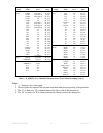
Table 3 – B_DDR3D_3A TLA Channel Grouping (cont’d.)
Notes:
1. ‘ # ‘ denotes a low-true signal
2. These signals are required for accurate acquisition and post-processing of acquired data
3. The ‘M’ in front of a TLA channel denotes the Master card of the merged set
4. The ‘S’ in front of a TLA channel denotes Slave card #1 of the merged set
5. The ‘S2’ in front of a TLA channel denotes Slave card #2 of the merged set
6. Signals in these groups are acquired using the TLA’s demux capability and will not have
a MagniVu display value