


DDR3THIN-MN-XXX 66 Doc. Rev. 1.11
data are displayed. Note that the timestamp is updated to reflect the time between displayed
cycles.
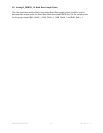
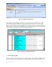
6.2 Viewing Raw DDR3 Data using B_DDR3D_XX Supports
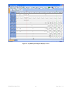
In order to make the display of DDR3 data more user-friendly the raw data from the Address, all
Data and other groups is suppressed in the B_DDR3D_2D Listing display. Instead the post-
processing display software formats and reorders the data to tag and display valid DDR3
Address, Commands and Data. In the case of the B_DDR3D_2D supports, which stores two
Read and two Write data cycles in each TLA Sample location, the data is reordered
chronologically in the display with the oldest data being shown on the line above the newer data.
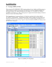
To see the raw data using the Interposer support package perform a right mouse click in the
Listing window, select
Add Column… then click on the group to be added. Refer to the TLA
User’s Manual or online help for further information on added or deleting data groups.
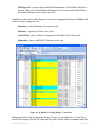
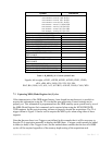
6.3 B_DDR3D_2A / 3A Mnemonics Description
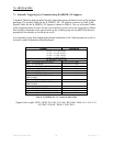
Table 6 gives a brief description of each of the text lines displayed in the B_DDR3D_2A / _3A
post-processing software display.
Mnemonic Description
ACT – BANK ACTIVATE (Sx#) Bank: Active command – activate a row in a bank for subsequent access
(Chip Select 0-3; Bank x)
DESL - IGNORE COMMAND Deselect function – no new command
(E)MRS – (EXTENDED) MODE
REGISTER SET x (Sx#)
Mode Register Set command, registers 0-3;
(Chip Select 0-3)
NOP - NO OPERATION (Sx#) No Operation command (Chip Select 0-3)
PRE – SINGLE BANK PRECHARGE (Sx#)
Bank:
Precharge command (Chip Select 0-3; Bank x)
PREA – PRECHARGE ALL BANK (Sx#) Precharge All command (Chip Select 0-3)
RDA – READ W/AUTO PRECHARGE
(Sx#) Bank:
Read command with auto precharge (Chip Select 0-3; Bank x)
RD - READ (Sx#) Bank: Read command – initiates a burst read access to active row
(Chip Select 0-3; Bank x)
READ DATA Valid Read data on the bus
REF - REFRESH (Sx#) Self Refresh command (Chip Select 0-3)
WRA – WRITE W/AUTO PRECHARGE
(Sx#) Bank:
Write command with auto precharge (Chip Select 0-3; Bank x)
WR - WRITE (Sx~) Bank: Write command – initiates a burst write access to active row
(Chip Select 0-3; Bank x)
WRITE DATA Valid Write data on the bus
ZQCL – ZQ CALIBRATION LONG (Sx#) ZQ Calibration Long (Chip Select 0-3)
ZQCS – ZQ CALIBRATION SHORT (Sx#) ZQ Calibration Short (Chip Select 0-3)
Table 6 - B_DDR3D_2A / 3A Mnemonics Definition
6.4 B_DDR3D_2G Mnemonics Description