


1999 Oct 12 10
Philips Semiconductors Product specification
IC card interface TDA8002C
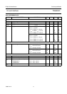
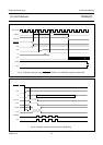
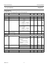
Table 1 Clock circuitry definition
Notes
1. X = don’t care.
2. In low-power mode.
3. f
int
= 32 kHz in low-power mode.
MODE CLKSEL CLKDIV1 CLKDIV2
FREQUENCYOF
CLK
FREQUENCYOF
CLKOUT
HIGH LOW HIGH LOW
1
⁄
2
f
int
1
⁄
2
f
int
HIGH LOW LOW LOW
1
⁄
4
f
xtal
f
xtal
HIGH LOW LOW HIGH
1
⁄
2
f
xtal
f
xtal
HIGH LOW HIGH HIGH STOP low f
xtal
HIGH HIGH X
(1)
X
(1)
STROBE f
xtal
LOW
(2)
X
(1)
X
(1)
X
(1)
STOP low
1
⁄
2
f
int
(3)
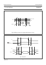
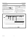
I/O circuitry
The three I/O transceivers are identical. Thestate is HIGH
for allI/O pins (i.e. I/O,I/OUC, AUX1, AUX1UC,AUX2 and
AUX2UC). Pin I/O is referenced to V
CC
and pin I/OUC to
V
DD
, thus ensuring proper operation in the event that
V
CC
≠ V
DD
.
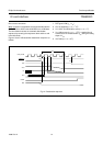
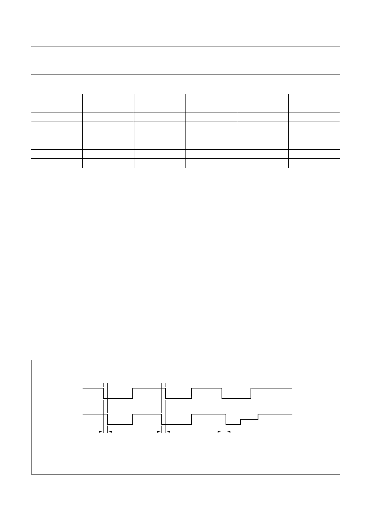
The first side on which a falling edge is detected becomes
a master (input). An anti-latch circuitry first disables the
detection of the falling edge on the other side, which
becomes slave (output), see Fig.8.
After a delay time t
d
(between 50 and 400 ns), the logic 0
present on the master side is transferred on the slave side.
When the input is back to HIGH level, a current booster is
turned on during the delay t
d
on the output side and then
both sides are back to their idle state, ready to detect the
next logic 0 on any side.
In the event of a conflict, both lines may remain LOW until
the software enables the lines to be HIGH. The anti-latch
circuitry ensures that the lines do not remain LOW if both
sides return HIGH, regardless of the prior conditions.
The maximum frequency on the lines is approximately
200 kHz.
When CS is HIGH, I/OUC, AUX1UC and AUX2UC are
internally pulled-up to V
DD
with 20 kΩ resistors. When
CS is LOW, I/OUC, AUX1UC and AUX2UC are
permanently HIGH (with integrated 100 kΩ pull-up
resistors connected to V
DD
).
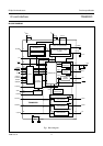
Fig.8 Master and slave signals.
handbook, full pagewidth
t
d
MGD703
t
d
t
d
I/O
I/OUC
conflict idle