


1999 Oct 12 16
Philips Semiconductors Product specification
IC card interface TDA8002C
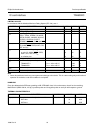
LIMITING VALUES
In accordance with the Absolute Maximum Rating System (IEC 134); note 1.
Note
1. Stress beyond these levels may cause permanent damage to the device. This is a stress rating only and functional
operation of the device under this condition is not implied.
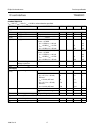
HANDLING
Every pin withstands the ESD test according to MIL-STD-883C class 3 for card contacts, class 2 for the remaining.
Method 3015 (HBM 1500 Ω, 100 pF) 3 positive pulses and 3 negative pulses on each pin with respect to ground.
THERMAL CHARACTERISTICS
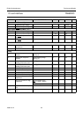
SYMBOL PARAMETER CONDITIONS MIN. MAX. UNIT
V
DDD
digital supply voltage −0.3 +6.5 V
V
DDA
analog supply voltage −0.3 +6.5 V
V
CC
card supply voltage pins;
XTAL1, XTAL2, ALARM, CS, MODE,
RSTIN, CLKSEL, AUX2UC, AUX1UC,
CLKDIV1, CLKDIV2, CLKOUT,
STROBE, CMDVCC, CV/TV and OFF
−0.3 +6.5 V
V
i(card)
input voltage on card contact pins;
I/O, AUX2, PRES,PRES, AUX1, CLK,
RST and V
CC
−0.3 +6.5 V
V
es
electrostatic handling voltage
on pins I/O, AUX2,
PRES, PRES,
AUX1, CLK, RST and V
CC
−6+6kV
on all other pins −2+2kV
T
stg
storage temperature −55 +125 °C
P
tot
continuous total power dissipation
TDA8002CT/x T
amb
= −25 to +85 °C − 0.56 W
TDA8002CG T
amb
= −25 to +85 °C − 0.46 W
T
amb
ambient temperature −25 +85 °C
T
j
junction temperature − 150 °C
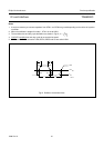
SYMBOL PARAMETER CONDITIONS VALUE UNIT
R
th(j-a)
thermal resistance from junction to ambient in free air
SOT136-1 70 K/W
SOT401-1 91 K/W