


1999 Oct 12 12
Philips Semiconductors Product specification
IC card interface TDA8002C
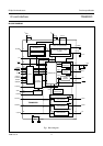
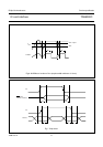
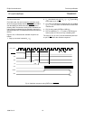
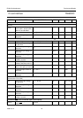
ACTIVATION SEQUENCE
From Idle mode, the circuit enters the activation mode
when the microcontroller sets the CMDVCC line LOW or
sets the MODE line HIGH when the CMDVCC line is
already LOW. The internal circuitry is then activated, the
internal clock is activated and an activation sequence is
executed. When RST is enabled it becomes the inverse of
RSTIN.
Figures 10 to 12 illustrate the activation sequence as
follows:
1. Step-up converter is started (t
1
≈ t
0
)
2. V
CC
rises from 0 to 3 or 5 V (t
2
=t
1
+1
1
⁄
2
T) (according
to the state on pin CV/TV)
3. I/O, AUX1 and AUX2 are enabled and CLKis enabled
(t
3
=t
1
+ 4T); I/O, AUX1 and AUX2 were forced LOW
until this time
4. CLK is set by setting RSTIN to HIGH (t
4
)
5. RST is enabled (t
5
=t
1
+ 7T); after t
5
, RSTIN has no
further action on CLK, but is only controlling RST.
The value of V
CC
(5 or 3 V) must be selected by the level
on pin CV/TV before the activation sequence.
Fig.10 Activation sequence using RSTIN and CMDVCC.
handbook, full pagewidth
FCE273
OSC_INT/64
CMDVCC
VUP
V
CC
I/O
CLK
RSTIN
RST
LOW
t
act
t
0
t
1
t
2
t
3
t
4
t
5
T = 25 µs