


1999 Oct 12 8
Philips Semiconductors Product specification
IC card interface TDA8002C
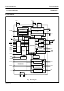
FUNCTIONAL DESCRIPTION
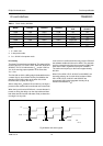
Power supply
The supply pins for the chip are V
DDA
, V
DDD
, AGND,
DGND1 and DGND2. V
DDA
and V
DDD
(i.e. V
DD
) should be
in the range of 3.0 to 6.5 V. All card contacts remain
inactive during power-up or power-down.
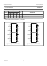
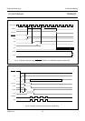
On power-up, the logic is reset by an internal signal.
The sequencer is not activated until V
DD
reaches
V
th2
+V
hys2
(see Fig.6). When V
DD
falls below V
th2
, an
automatic deactivation sequence of the contacts is
performed.
Chip selection
The chip select pin (CS) allows the use of several
TDA8002Cs in parallel.
When CS is HIGH, the pins RSTN, CMDVCC, MODE,
CV/TV, CLKDIV1, CLKDIV2, CLKSEL and STROBE
control the chip, pins I/OUC, AUX1UC and AUX2UC are
the copy of I/O, AUX1 and AUX2 when enabled (with
integrated 20 kΩ pull-up resistors connected to V
DD
) and
OFF is enabled.
When CS goes LOW, the levels on pins RSTIN,
CMDVCC, MODE, CV/TV, CLKDIV1, CLKDIV2 and
STROBE are internally latched, I/OUC, AUX1UC and
AUX2UC go to high-impedance with respect to I/O, AUX1
and AUX2 (with integrated 100 kΩ pull-up resistors
connected to V
DD
) and OFF is high-impedance.
Supply voltage supervisor (V
DD
)
This block surveys the V
DD
supply. A defined retriggerable
pulse of 10 ms minimum (t
W
) is delivered on the ALARM
output during power-up or power-down of V
DD
(see Fig.6).
This signal is also used for eliminating the spikes on card
contacts during power-up or power-down.
When V
DD
reaches V
th2
+V
hys2
, an internal delay (t
W
) is
started. The ALARM output is active until this delay has
expired. When V
DD
falls below V
th2
, ALARM is activated
and a deactivation sequence of the contacts is performed.
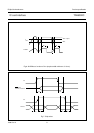
Clock circuitry
The TDA8002C supports both synchronous and
asynchronous cards. Thereare three methodsto clock the
circuitry:
• Apply a clock signal to pin STROBE
• Use of an internal RC oscillator
• Use of a quartz oscillator which should be connected
between pins XTAL1 and XTAL2 or an external clock
applied on XTAL1.
When CLKSEL is HIGH,the clock should be appliedto the
STROBE pin. When CLKSEL is LOW, the internal
oscillators is used.
When an internal clock is used, the clock output is
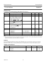
available on pinCLKOUT. The RC oscillator is selected by
making CLKDIV1 HIGH and CLKDIV2 LOW. The clock
output to the card is available on pin CLK. The frequency
of the card clock can be the input frequency divided by
2 or 4, STOP low or 1.25 MHz, dependingon the states of
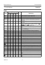
CLKDIV1 or CLKDIV2 (see Table 1).
When STROBE is used for entering the clock to a
synchronous card, STROBE should remain stable during
activation sequence otherwise the first pulse may be
omitted.
Do not change CLKSEL during activation. When in
low-power (sleep) mode, the internal oscillator frequency
which is available on pin CLKOUT is lowered to
approximately 16 kHz for power economy purposes.