


- 31 -
nVIDIA MCP73 Series Users Manual
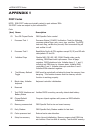
•
Back to Frequency/Voltage Control Setup Menu
・
BIOS Write Protect
Available options: [Disabled], [Enabled].
・
Onboard Lan Control
Available options: [Disabled], [Enabled].
・
Lan BootROM Control
Available options: [Disabled], [Enabled].
・
DRAM Voltage Control
This option is for setting the voltage of DIMM.
・
CPU Voltage Control
This option is for setting the voltage of CPU.
・
Chipset Voltage Control
This option is for setting the voltage of Chipset.
・
CPUFSB Voltage Control
This option is for setting the voltage of CPUFSB.
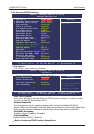
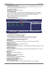
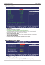
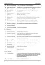
Phoenix - AwardBIOS CMOS Setup Utility
FSB & Memory Config
Parameters
Current CPU Freq, MHz
FSB Clock, MHz
CPU Multiplier
FSB - Memory Clock Mode
x FSB - Memory Ratio
x FSB (QDR), MHz
Actual FSB (QDR), MHz
x MEM (DDR), MHz
Actual MEM (DDR), MHz
Setting
2666.7
533.3
20X
[Auto]
Auto
Auto
533.3
Auto
666.7
Current Value
2666.7
533.3
20X
533.3
666.7
Item Help
Menu Level
►
►
Memory Timing Setting [Press Enter]
↑↓
→←
:Move Enter:Select +/-/PU/PD:Value F10:Save ESC:Exit F1:General Help
F5: Previous Values F6: Fail-Safe Defaults F7: Optimized Defaults
Auto
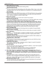
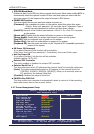
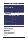
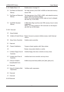
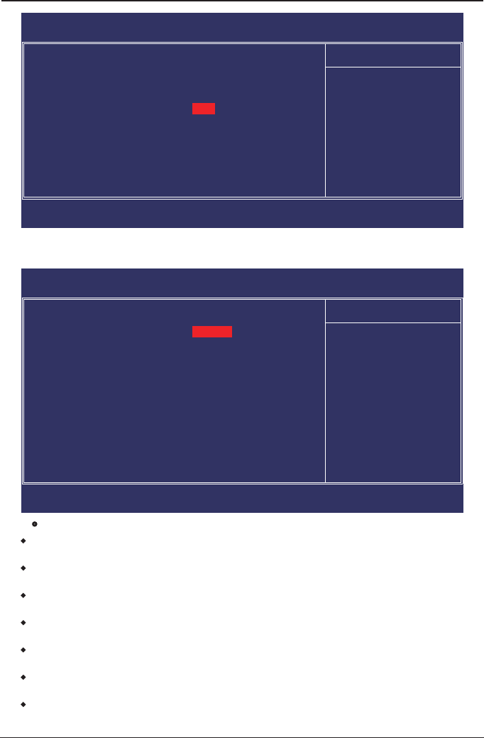
Phoenix - AwardBIOS CMOS Setup Utility
Memory Timing Setting
Parameters
Memory Timing Setting
x tCL (CAS Latency)
x tRCD
x tRP
x tRAS
x Command Per Clock (CMD)
Setting
[Optimal]
Auto(0)
Auto(0)
Auto(0)
Auto(0)
Auto(0T)
Current Value
5
5
5
15
2T
Item Help
Menu Level
►
** Advanced Memory Settings **
x tRRD
x tRC
x tWR
x tWTR
x tREF
Auto(0)
Auto(0)
Auto(0)
Auto(0)
Auto
3
20
5
11
7.8uS
↑↓
→←
:Move Enter:Select +/-/PU/PD:Value F10:Save ESC:Exit F1:General Help
F5: Previous Values F6: Fail-Safe Defaults F7: Optimized Defaults
Optimal
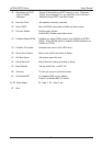
►
Memory Timing Setting
Click <Enter> key to enter its submenu:
Use this menu to set optimal timings or to manually enter timings.