


M301N2T-PRB User’s Manual 4. Hardware Specifications
REJ10J0037-0100 Rev.1.00 Mar.16, 2005
Page 33 of 48
4.2 Differences between the Actual MCU and Emulator
Differences between the actual MCU and emulator are shown below. When debugging the MCU using this product, be careful
about the following precautions.
IMPORTANT
Note on Differences between the Actual MCU and Emulator:
Operations of the emulator system differ from those of actual MCUs as listed below.
(1) Reset condition
Set the time for starting up (0.2 Vcc to 0.8 Vcc) 1 μs or less.
(2) Initial values of internal resource data of an MCU at power-on
(3) Internal memories (ROM and RAM) capacities etc.
With this emulator system, regardless of ROM and RAM of the MCU you use, all the areas other
than the SFR area can be read and written into.
(4) Oscillator circuit
- In the oscillator circuit where an oscillator is connected between pins X
IN
and X
OUT
, oscillation
does not occur because a flexible cable, buffer IC and other devices are used between the
evaluation MCU and the user system. It is same for the sub-clock oscillation circuit (pins X
CIN
and X
COUT
).
- For notes on when using the oscillator circuit on the user system, refer to "2.1.3 Using the
Oscillator Circuit on the User System" (page 18).
(5) A/D converter function
Because a flexible cable and other devices are used between the evaluation MCU and the user
system, the A/D converter operates differently from that of the actual MCU.
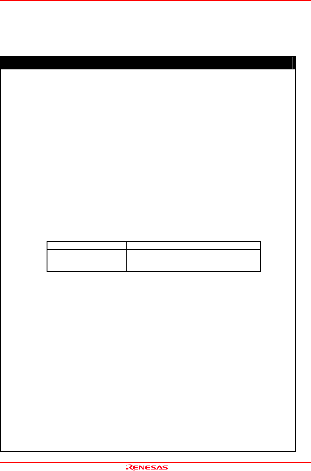
(6) DBC, single-step and BRK instruction interrupt vector table addresses
Although data can be downloaded to the DBC, single-step, or BRK instruction interrupt vector
table addresses, be aware that because the emulator system uses this area, the data read from this
area may not be an expected value (see Table 4.2).
Table 4.2 Vector table addresses for the emulator
Factor of interruption Vector table addresses Data read
DBC*1 FFFF4h--FFFF7h Indefinite
Single-step*1 FFFECh--FFFEFh Indefinite
BRK instruction FFFE4h--FFFE7h Indefinite
*1 Interruption for the emulator only
(7) Pin X
OUT
Pin X
OUT
is not assigned to the evaluation MCU used by this product. For this reason, pin X
OUT
of
this product is open.
(8) Pin IVCC
Pin IVCC of this product is open. The circuit for IVCC on this product is connected to pin IVCC
on the evaluation MCU.
(9) Timer X
When the device is to be operated in pulse period measurement mode, be sure to use timer C.
(10) Timer Z
When operating in programmable wait one-shot generation mode, an invalid interrupt may be
generated at the end of TZOUT waveform output. Please do not use programmable wait one-shot
generation mode of timer Z.
(11) Timer C
To measure the frequency of the on-chip oscillator, be sure to use timer Y.
(12) INT1, 2, 3
- To clear the INT input enable bit to 0, set the interrupt priority level to 0 before setting the INT
input enable bit to 0.
- To set the direction register for the corresponding port to 1, set the interrupt priority level to 0
before setting the direction register value to 1.
Note on NMI* Input:
"L" level input from the user system to pin NMI* is accepted only while a user program is being
executed (only while the RUN status LED on the PC4701's front panel is lit).