


( 29 / 40 )
6. Precautions to Be Taken When Debugging
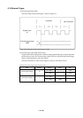
6.1 Reset
The M34551T2-MCU uses 74AC14 for the reset signal input buffer, and electrical characteristics
therefore differ from those of an actual chip.
Table 6.1 lists the RESET signal input characteristics on the M34551T2-MCU.
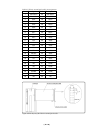
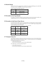
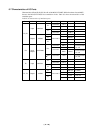
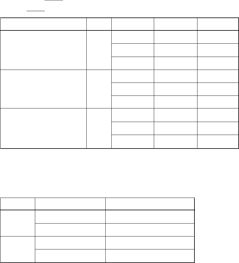
Table 6.1 RESET signal input characteristics
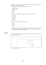
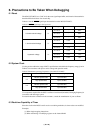
6.2 System Clock
Use the product within the range of MCU specifications and within the frequency range given in
Table 6.2 in accordance with power source voltage and operation mode.
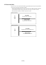
Table 6.2 Maximum operating frequencies of the M34551T2-MCU
Item
H-level threshold voltage
L-level threshold voltage
Hysteresis voltage
Symbol
VP
VN
VH
Voltage
VCC=3.0 V
VCC=4.5 V
VCC=5.5 V
VCC=3.0 V
VCC=4.5 V
VCC=5.5 V
VCC=3.0 V
VCC=4.5 V
VCC=5.5 V
Min.
-
-
-
0.5 V
0.9 V
1.1 V
0.3 V
0.4 V
0.5 V
Max.
2.2 V
3.2 V
3.9 V
-
-
-
1.2 V
1.4 V
1.6 V
Voltage
3 V
5 V
Mode
Medium-speed mode
High-speed mode
Medium-speed mode
High-speed mode
Maximum operating frequency
Up to 4.0 MHz
Up to 1.0 MHz
Up to 8.0 MHz
Up to 2.0 MHz
Use components required for the OSC-2 oscillator circuit board (included) if changing frequency in
accordance with the target system.
For details about the oscillation circuit constants, consult the manufacturer of your oscillator.
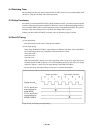
6.3 Real-time Capability of Timer
Since the clock on the MCU board is active even during emulation, its timer values are modified.
Examples:
(1) When single-stepping instructions
(2) When referencing or modifying registers or the internal RAM