


( 30 / 40 )
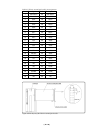
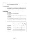
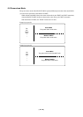
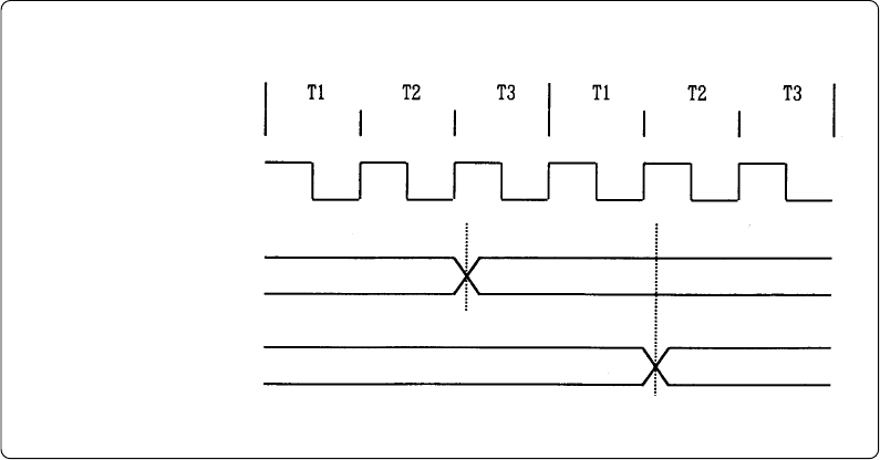
Figure 6.1 P0, P1 and D port output timings
P0, P1, and D port
output timings on
M34551T2-MCU
Next output instruction
Output instruction
System clock X
IN
P0, P1, and D port
output timings on
actual MCUs
6.4 Watchdog Timer
The watchdog timer does not operate on the M34551T2-MCU board. Use an evaluation MCU (OTP
version) to verify the watchdog timer-related operations.
6.5 Pullup Transistors
Since the P1 port of the M34551T2-MCU contains emulation circuits, you cannot control the pullup
transistors using the pullup control register PU0. When you want to use the internal pullup transistors,
turn on switches SW4 to SW7 to activate the pullup resistors of the M34551T2-MCU. The port P1's
resistance value of the pullup resistor is 68 kΩ by the settings (SW4 to SW7).
And the port P0's (M34551T2-MCU) resistance value of the pullup register is 68 kΩ.
6.6 Port I/O Timing
(1) Port input timing
Port input timings are the same as with the actual MCUs.
(2) Port output timing
When using the M34551T2-MCU, output timings are different from those of the actual MCUs
for the following ports that are configured with port emulation circuits:
• Ports P00 to P03
• Ports P10 to P13
• Ports D0 to D5
With the actual MCUs, changes occur at the beginning of the T3 state of an output instruction.
With the M34551T2-MCU, changes occur at the beginning of the T2 state of the next output
instruction. Figure 6.1 shows the port output timings of the M34551T2-MCU.
For the other ports, the output timings are the same as with the actual MCUs.