


Features and Specifications
2.3.2 Flash Memory S29GL032A90TFIR4 (Standard component)
Rev.1.01
Oct 28, .2008 2-5
REJ10J1351-0101
2
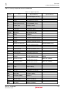
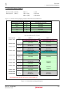
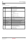
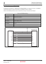
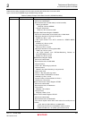
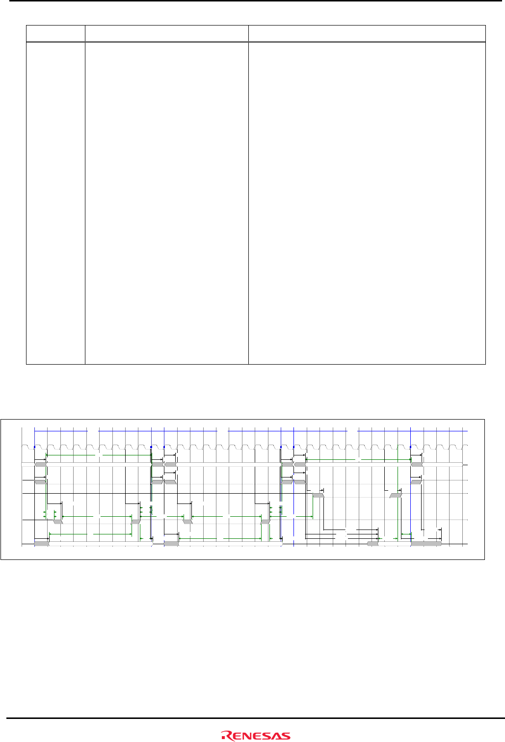
Table 2.3.2 Setting Example of Bus State Controller (Flash Memory Write and Read)
User Area Applicable Device Settings for Bus State Controller
CS0 S29GL032A90TFIR4 CS0 Space Bus Control Register: CS0BCR
Initial value: H'36DB 0400 (MD3 = "L")
Recommended value: H'1000 0400
• Idle Cycles between Write-Read Cycles and
Write-Write Cycles
IWW[1:0] = B'01: 1 idle cycle inserted
• Data bus width
BSZ[1:0] = B’10: *Shall be ignored.
CS0 space wait control register: CS0WCR
Initial value: H'0000 0500
Recommended value: H'0000 0AC1
• Number of Delay Cycles from address, CS0#
Assertion to RD#, WEn#
SW[1:0] = B'01; 1.5 cycles
• Number of Access Wait Cycles
WR[3:0] = B'0101; 5 cycles
• Ignore external WAIT input
WM = B’1;
• Number of Delay Cycles from RD#, WEn# negation
to address, CS0# negation
HW[1:0] = B'01; 1.5 cycles
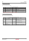
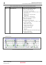
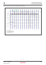
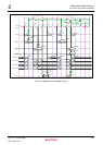
<Write/Read Timing>
Write1 Write2 Read1
DATA DATA DATA
tDF(OE)
tDF(CE)
ta(CE1)
ta(AD)
ta(OE)
tWDH1
tWDD1
tWDH1tWDD1
tWED1tWED1tWED1tWED1
tRSDtRSD
tCSD1
tCSD1
tCSD1
tCSD1
tCSD1tCSD1
tAD1tAD1
tAD1
tAD1
tAD1tAD1
tRDH1
tRDS1tDHtDStDH
tDS
tOEH
tAH
tCH
tWPtWPH tWP
tAH
tWPH
tCH
tWPtAS
tCS
tWP
tRCtRC
tWCtWC
T1T2Tw4T1 Tw 1 Tw 2 Tw 1 Tw 2 T2 T1 Tw 1 Tw2 Tw 3 T2Tf Tf Taw 1Taw 1Th Th Th TfTw 4Tw 3 Tw 3 Tw 4 Tw 5Tw 5 Tw 5
CKIO
A
21-A1
CS0#
RD#
WE0#
D15-D0
Figure 2.3.2 Flash Memory Read and Write Access Timing Example