


Features and Specifications
2.3.3 External Synchronous DRAM
Rev.1.01
Oct 28, .2008 2-7
REJ10J1351-0101
2
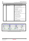
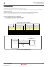
A power-on sequence is required to use a SDRAM. Power-on sequence is to initialize the pin function controller (PFC),
set registers in the bus state controller and write data in the SDRAM mode register.
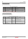
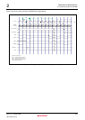
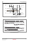
Table 2.3.4 lists the access address when writing in the SDRAM mode register on the CS3 space.
Table 2.3.4 Access Address for SDRAM Mode Register Write (CS3 Space)
Burst read/single write (burst length 1) Burst read/burst write (burst length 1)
Data bus
width
CAS
latency
Access Address External Address Pin Access Address External Address Pin
16 bits 2 H'F8FD 5440 H'0000 0440 H'F8FD 5040 H'0000 0040
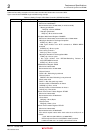
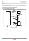
Execute following settings to the M3A-HS19 SDRAM mode register.
• Burst length: Burst read/single write (burst length 1)
• Wrap type: Sequential
• CAS latency: 2 cycles
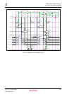
To write data in the SDRAM mode register as shown in Table 2.3.4, write the arbitrary data in words to the address of
H'F8FD 5440 (the data in this case is ignored). Following commands are sequentially issued to the SDRAM by the word
writing.
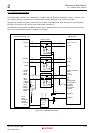
1.All banks precharge command (PALL)
Idle cycles (Tpw), of which number is specified by bits WTRP1 and WTRP0 in CS3WCR, are inserted between the PALL
and the first REF commands.
2. Auto-refreshing command (REF) for eight times
Idle cycles (Trc), of which number is specified by bits WTRP1 and WTRP0 in CS3WCR are inserted after issuing REF
command
3. Mode register write command (MRS)