


Operational Specifications
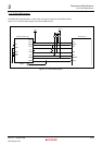
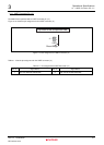
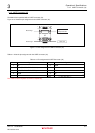
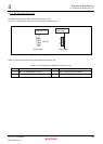
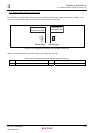
3.1.4 PCMCIA Connector (J4)
Rev.1.01
Oct.28.2008 3-7
REJ10J1351-0101
3
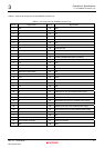
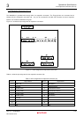
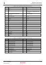
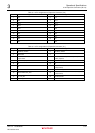
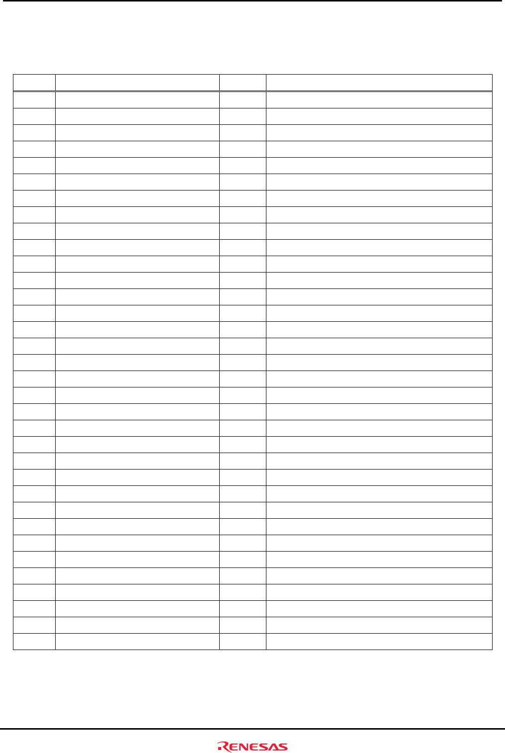
Table 3.1.4 lists the pin assignment for the PCMCIA connector (J4).
Table 3.1.4 Pin assignment for PCMCIA Connector (J4)
Pin no. Signal Name Pin no. Signal Name
1 GND 35 GND
2 D3 36 CD1# (PC15/CRS)
3 D4 37 D11
4 D5 38 D12
5 D6 39 D13
6 D7 40 D14
7 CE1# (CE2A#) 41 D15
8 A10 42 CE2# (CE1A#)
9 OE# (RD#) 43 VS1# (Pulled up to the PCMCIA power supply)
10 A11 44 IORD# (PB05/WE2#/DQMUL/ICIORD#)
11 A9 45 IOWR# (PB06/WE3#/DQMUU/ICIOWR#)
12 A8 46 A17
13 A13 47 A18
14 A14 48 A19
15 WE# (WE1#/DQMLU/WE#) 49 A20
16 IREQ# (PD7/IRQ7/SCK2) 50 A21
17 VCC 51 VCC
18 VPP1 52 VPP2
19 A16 53 A22
20 A15 54 A23
21 A12 55 A24
22 A7 56 A25
23 A6 57 VS2# (Pulled up to the PCMCIA power supply)
24 A5 58 RESET (PC09/RX_ER)
25 A4 59 WAIT# (PB00/WAIT#)
26 A3 60 INPACK# (Pulled up to the PCMCIA power supply)
27 A2 61 REG# (PC14/COL)
28 A1 62 SPKR# (Pulled up to the PCMCIA power supply)
29 A0 63 STSCHG# (Pulled up to the PCMCIA power supply)
30 D0 64 D8
31 D1 65 D9
32 D2 66 D10
33 IOIS16#
(PB01/IOIS16#)
67 CD2# (PC15/CRS)
34 GND 68 GND