


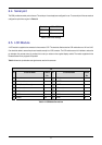
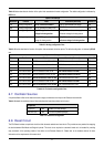

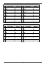
Table 6-9 below describes the function of the option links associated with serial configuration. The default configuration is indicated by
BOLD text.
Option Link Settings
Reference Function Fitted Alternative (Removed) Related To
R36 Analog configuration
PIN 57 connected to ADPOT
PIN 57 disconnected from ADPOT R66
R66 Analog configuration PIN 57 connected to AN8 on JA5
PIN 57 disconnected from AN8
R36
R40 Analog configuration
UC_VCC supplies the reference
voltage for Analog section.
CON_VREF can be used to supply the
reference voltage for Analog section.
R41
R41 Analog configuration CON_VREF supplies the reference
voltage for Analog section.
UC_VCC can be used to supply the
reference voltage for Analog section.
R40
Table 6-9: Analog configuration links
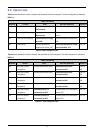
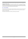
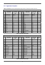
Table 6-10 below describes the function of the option links associated with other options. The default configuration is indicated by BOLD
text.
Option Link Settings
Reference Function Fitted Alternative (Removed) Related To
R49 Pin function select
PIN 76 connected to AN0 on JA1
PIN 76 disconnected from on JA1 R58
R58 Pin function select PIN 76 connected to DA1 on JA1
PIN 76 disconnected from DA1
R49
R56 Pin function select
PIN 74 connected to AN1 on JA
PIN 74 disconnected from AN1 on JA R59
R59 Pin function select PIN 74 connected to DA0 on JA
PIN 74 disconnected from DA0
R56
R63 Pin function select PIN 46 connected to INT3n on JA1
PIN 46 disconnected from INT3n
R67
R67 Pin function select
PIN 46 connected to RXD1 on JA6
PIN 46 disconnected from RXD1 R63
R57 Pin function select PIN 73 connected to AN2 on JA1
PIN 73 disconnected from AN2
R62
R62 Pin function select
PIN 73 connected to CLK1 on JA6
PIN 73 disconnected from CLK1 R57
Table 6-10: Pin function configuration links
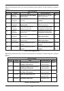
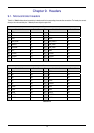
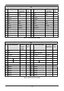
6.7. Oscillator Sources
A crystal oscillator is fitted on the board and used to supply the main/sub clock input to the Renesas microcontroller.
Table 6-10 details the oscillators that are fitted and alternative footprints provided on this board:
Component
Crystal (X1) Fitted 20 MHz (HC/49U package)
Sub clock (X2) Fitted 32.768 kHz (90SMX package)
Table 6-10: Oscillator Configuration
6.8. Reset Circuit
The CPU Board includes a simple latch circuit that links the mode selection and reset circuit. This provides an easy method for swapping
the device between Boot Mode and Single chip mode. This circuit is not required on customers’ boards as it is intended for providing
easy evaluation of the operating modes of the device on the Renesas Starter Kit. Please refer to the hardware manual for more
information on the requirements of the reset circuit.
11