


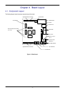

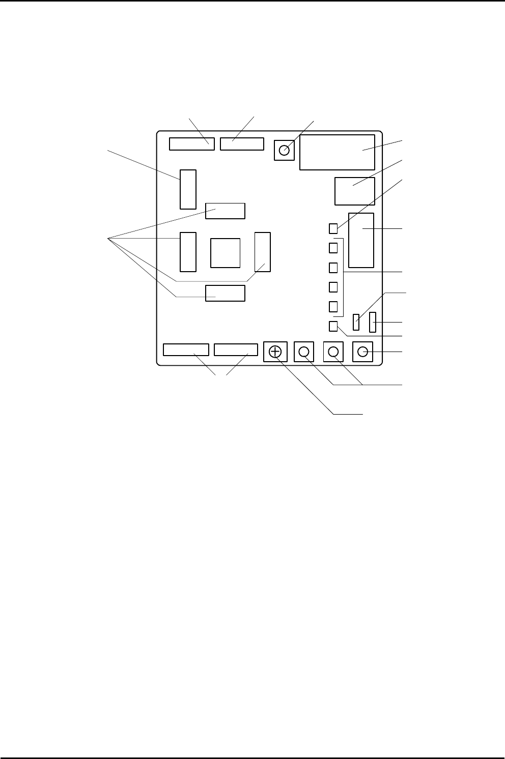
Chapter 4. Board Layout
4.1. Component Layout
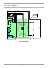
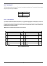
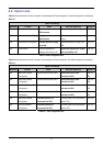
The following diagram shows the top layer component layout of the board.
JA6
MCU
Reset Switch
E8 Header
User Switches
Potentiometer
User LED
Power LED
Boot LED
Powe
r
A
pplication Board Interface
Microcontroller Pin Headers
(J1 to J4)
LCD Display
A
pplication Board Interface
RS232 Serial
User/Boot Switch
LIN Connecto
r
Power Connecto
r
for LIN
JA2
JA5 JA1
Figure 4-1: Board Layout
4