


UX-258TH
FO-475TH
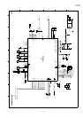
[4] Circuit description of power supply PWB
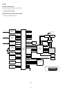
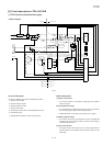
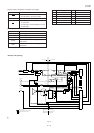
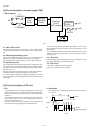
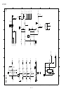
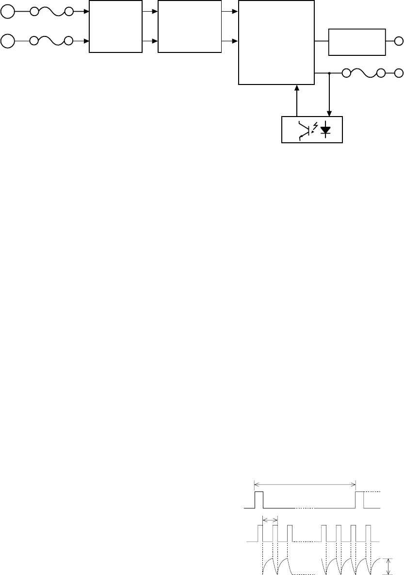
1. Block diagram
2-1. Noise filter circuit
The input noise filter section is composed of L and C, which reduces
normal mode noise from the AC line and common mode noise to the AC
line.
2-2. Rectifying/smoothing circuit
The AC input voltage is rectified by diode D1, 2, 3, 4 and smoothed by
capacitor C5 to supply DC voltage to the switching circuit section.
Power thermistor TH1 suppresses inrush current at power switch-on.
2-3. Switching circuit
This circuit employs the self excited ringing choke convertor (RCC) sys-
tem. In this system, the DC voltage supplied from the rectifying/smooth-
ing section is converted into high frequency pulses by ON/OFF repeti-
tion of MOS FET Q1.
Energy is charged in the primary winding of T1 during ON period of Q1,
and discharged to the secondary winding during OFF period.
The output voltage is controlled by adjusting ON period of Q1 which
changes charge time of C9 through operation of photo-coupler PC1 from
+24V output.
[5] Circuit description of CIS unit
1. CIS
Cis is an image sensor which puts the original paper in close contact
with the full-size sensor for scanning, being a monochromatic type
with the pixel number of 1,728 dots and the main scanning density of
8 dots/mm.
It is composed of sensor, rod lens, LED light source, light-conductive
plate, control circuit and so on, and the reading line and focus are
previously adjusted as the unit.
Due to the full-size sensor, the focus distance is so short that the set
is changed from the light weight type to the compact type.
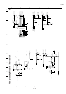
Fig. 8
Fig. 7
The overcurrent protection is performed by bringing Q1 to OFF state
through detection of voltage increase in the auxiliary winding of T1 by
ZD2 and R9.
The overvoltage protection is performed by operating the overcurrent
protection circuit through destruction of zener diode ZD4 and short-
circuiting of load.
2-4. +5V circuit
Each DC voltage supplied by rectifying the output of transformer T1 with
diode D8 is stabilized by 3-terminal regulator IC1.
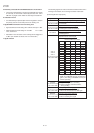
2-5. VTH circuit
VTH output is supplied through the relay RY1.
Relay RY1 is operated by VTH-ON signal.
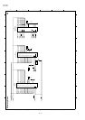
5ms
2µs
0V
2V(TYP)
(White original paper)
Approx.5V
øT
CISCLK
VO
5 – 11
2. Waveforms
The following clock is supplied from FC200 of the control board, and
VO is output.
Noise
Filter
Circuit
Rectifying
Smoothing
Circuit
Switching
Circuit
(RCC system)
Regulater
Circuit
+5V
+24V
AC IN
Photo Coupler
F1
T1.25A/250V
F3
4A/72V
F2
T1.25A/250V