


TABLE OF CONTENTS SSD-CXXX(I)-3150 DATA SHEET
SILICONSYSTEMS PROPRIETARY
This document and the information contained within it is confidential and proprietary to SiliconSystems, Inc.
All unauthorized use and/or reproduction is prohibited.
3150C-10DSR PAGE IV FEBRUARY 2, 2009
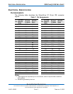
True IDE Multiword DMA Read/Write Access Timing .......................................... 21
Attribute Memory Description and Operation........................................................... 22
Attribute Memory Read Operations............................................................................ 22
Attribute Memory Write Operations............................................................................ 23
Attribute Memory Map................................................................................................ 24
Card Information Structure......................................................................................... 25
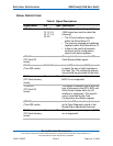
Configuration Option Register (200h)......................................................................... 36
Configuration and Status Register (202h).................................................................. 37
Pin Placement Register (204h) .................................................................................. 38
Socket and Copy Register (206h) .............................................................................. 39
Common Memory Description and Operation .......................................................... 40
Common Memory Read Operations........................................................................... 40
Common Memory Write Operations........................................................................... 40
I/O Space Description and Operation ........................................................................ 41
I/O Space Read Operations ....................................................................................... 41
I/O Space Write Operations ....................................................................................... 41
ATA and True IDE Register Decoding ........................................................................ 42
Memory-Mapped Register Decoding.......................................................................... 42
Independent I/O Mode Register Decoding................................................................. 43
Primary and Secondary I/O Mapped Register Decoding ........................................... 44
Task File Register Specification................................................................................. 45
ATA Registers............................................................................................................... 46
Data Register ............................................................................................................. 46
Error Register............................................................................................................. 46
Feature Register......................................................................................................... 47
Sector Count Register................................................................................................ 48
Sector Number Register............................................................................................. 49
Cylinder Low Register ................................................................................................ 50
Cylinder High Register ............................................................................................... 51