


ATTRIBUTE MEMORY DESCRIPTION AND OPERATION SSD-CXXX(I)-3150 DATA SHEET
SILICONSYSTEMS PROPRIETARY
This document and the information contained within it is confidential and proprietary to SiliconSystems, Inc.
All unauthorized use and/or reproduction is prohibited.
3150C-10DSR PAGE 31 FEBRUARY 2, 2009
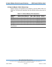
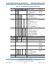
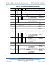
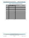
B6h 55h X Mantissa Exponent Nominal voltage = 5V V
CC
nominal value
B8h 4Dh X Mantissa Exponent V
CC
nominal 4.5V V
CC
minimum value
BAh 5Dh X Mantissa Exponent V
CC
nominal 5.5V V
CC
maximum value
BCh 75h X Mantissa Exponent Maximum average current over 10ms is
80mA
Maximum average
current
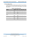
BEh EAh R S E I O AddrLine • R = 1: Range follows
• S = 1: 16-bit hosts supported
• E = 1: 8-bit hosts supported
IO AddrLines: 10 lines decoded
I/O space
description field
TPCE_IO
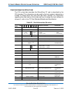
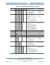
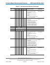
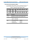
C0h 61h LS AS N Range • LS = 1: Size of lengths is 1 byte
• AS = 2: Size of address is 2 bytes
• N Range = 1: Address Range-1
I/O range format
description
C2h F0h First I/0 Base Address First I/O base address (LSB) First I/O range
address
C4h 01h First I/0 Base Address First I/O base address (MSB) -
C6h 07h First I/0 Base Address First I/O length -1 First I/O range
length
C8h F6h Second I/O Base Address Second I/O base address (LSB) Second I/O range
address
CAh 03h Second I/O Base Address Second I/O base address (MSB)
CCh 01h Second I/O Range Length Second I/O length -1 Second I/O range
length
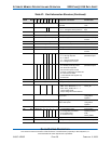
CEh EEh S P L M IRQ Level • S = 1: Share logic active
• P = 1: Pulse mode IRQ supported
• L = 1: Level mode IRQ supported
• M = 0: Bit mask of IRQs present —
IRQ level is IRQ14
Interrupt request
description structure
TPCE_IR
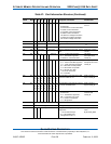
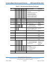
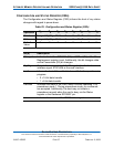
D0h 21h X R P R O A T - • X = 0: No more miscellaneous fields
•R: Reserved
• P = 1: Powerdown supported
• RO = 0: Not read only mode
• A = 0: Audio not supported
• T = 0: Single drive
Miscellaneous
features field
TPCE_MI
D2h 1Bh CISTPL_TABLE_ENTRY Configuration table entry tuple Tuple code
D4h 06h TPL_LINK Link length is 6 bytes Link to next tuple
D6h 02h I D Configuration Index ATA primary I/O mapped configuration
• I = 0: No Interface byte
• D = 0: No Default entry
• Configuration index = 2
Configuration table
index byte
TPCE_INDX
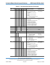
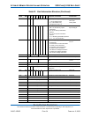
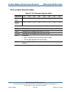
D8h 01h I D Configuration Index Contiguous I/O mapped ATA registers
configuration
• I = 0: No interface byte
• D = 0: No default entry
• Configuration index = 1
Configuration table
index byte
TPCE_INDX
Table 21: Card Information Structure (Continued)
Attribute
Offset
Data 7 6 5 4 3 2 1 0 Description of Contents CIS Function