


ATA AND TRUE IDE REGISTER DECODING SSD-CXXX(I)-3150 DATA SHEET
SILICONSYSTEMS PROPRIETARY
This document and the information contained within it is confidential and proprietary to SiliconSystems, Inc.
All unauthorized use and/or reproduction is prohibited.
3150C-10DSR PAGE 42 FEBRUARY 2, 2009
ATA AND TRUE IDE REGISTER DECODING
SiliconDrive can be configured as either a a memory-mapped or an an I/O
devices. As noted earlier, communication to and from the drive is
accomplished using the ATA Command Block.
MEMORY-MAPPED REGISTER DECODING
In memory-mapped mode, the SiliconDrive registers are accessed via
standard memory references (i.e., OE# and WE#). The ATA registers are
mapped to common memory space in a 2KB window starting at address 0.
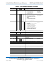
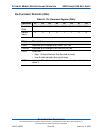
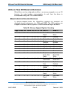
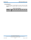
Table 30: Memory-Mapped Register Decoding
Reg# Offset A10 A9:A4 A3 A2 A1 A0 OE# = L WE# = L
1 0 0 X 0000Even Data
Read
Even Data
Write
1 1 0 X 0 0 0 1 Error Feature
1 2 0 X 0010Sector CountSector Count
1 3 0 X 0011Sector
Number
Sector
Number
1 4 0 X 0 1 0 0 Cylinder Low Cylinder Low
1 5 0 X 0 1 0 1 Cylinder High Cylinder High
1 6 0 X 0 1 1 0 Drive/Head Drive/Head
1 7 0 X 0111Status Command
1 8 0 X 1 0 0 0 Duplicate
Even Data
Read
Duplicate
Even Data
Write
1 9 0 X 1 0 0 1 Duplicate Odd
Data Read
Duplicate Odd
Data Write
1 D 0 X 1 1 0 1 Duplicate
Error
Duplicate
Feature
1 E 0 X 1 1 1 0 Alternate
Status
Device Control
1 F 0 X 1 1 1 1 Drive Address Reserved
1 X 1 X XXX0Even Data
Read
Even Data
Write
1 X 1 X XXX1Odd Data
Read
Odd Data
Write