ELECTRICAL SPECIFICATION SSD-DXXX(I)-4210 DATA SHEET
SILICONSYSTEMS PROPRIETARY
This document and the information contained within it is confidential and proprietary to SiliconSystems, Inc.
All unauthorized use and/or reproduction is prohibited.
4210D-03DSR PAGE 10 FEBRUARY 2, 2009
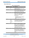
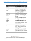
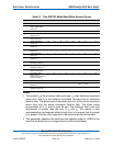
IORDY
(True IDE
mode)
27 I I/O Channel Ready. The signal is negated
to extend the host transfer cycle of any host
register access.
-IORD
(True IDE
mode)
25 I Device I/O Read. This is the read strobe
signal from the host. The falling edge of
IORD enables data from the device onto
the data bus. The rising edge of IORD
latches data at the host. The host does not
act on the data until it is latched.
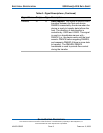
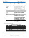
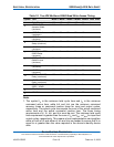
-DDMARDY
(UDMA write
protocol
active)
When UDMA mode DMA write is active in
all modes, this signal is asserted by the
device during a data burst to indicate that
the device is ready to receive UDMA data-
out bursts.
The device may negate -DDMARDY to
pause a UDMA transfer.
DSTROBE
(UDMA read
protocol
active)
When UDMA mode DMA read is active in
all modes, this signal is the data in strobe
generated by the device. Both the rising
and falling edge of DSTROBE cause data
to be latched by the host. The device may
stop generating DSTROBE edges to pause
a UDMA data-in burst.
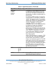
-IOWR
(True IDE
mode)
23 I Device I/O Write. This is the write strobe
signal from the host. The rising edge of
IOWR# latches data from the data bit
signals. The device does not act on the
data until it is latched.
-HDMARDY
(UDMA read
protocol
active)
When UDMA mode DMA read is active in
all modes, this signal is asserted by the
host to indicate that the host is ready to
receive UDMA data-in bursts. The host may
negate -HDMARDY to pause a UDMA
transfer.
Table 8: Signal Descriptions (Continued)
Signal Name Pin(s) Type Description


