


ELECTRICAL SPECIFICATION SSD-DXXX(I)-4210 DATA SHEET
SILICONSYSTEMS PROPRIETARY
This document and the information contained within it is confidential and proprietary to SiliconSystems, Inc.
All unauthorized use and/or reproduction is prohibited.
4210D-03DSR PAGE 24 FEBRUARY 2, 2009
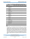
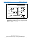
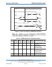
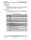
Figure 15: Device Terminating a UDMA Data-Out Burst
Note: The definitions for the DIOW-:STOP, IORDY:DDMARDY-
:DSTROBE, and DIOR-:HDMARDY-:HSTROBE signal lines are no longer
in effect after DMARQ and DMACK are negated.
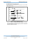
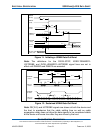
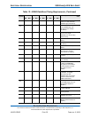
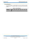
Table 13: UDMA Data Burst Timing Requirements
Symbol
Mode 0 Mode 1 Mode 2 Mode 3 Mode 4
Comment (see Notes 1 and
2)
Units
Min. Max. Min. Max. Min. Max. Min. Max. Min. Max.
t
2CYCTYP
240 - 160 - 120 - 90 - 60 - Typical sustained average
two-cycle time.
ns
t
CYC
112 - 73 - 54 - 39 - 25 - Cycle time allowing for
asymmetry and clock
variations (from STROBE
edge to STROBE edge).
ns
t
2CYC
230 - 154 - 115 - 86 - 57 - Two-cycle time allowing for
clock variations (from rising
edge to next rising edge, or
from falling edge to next
falling edge of STROBE).
ns
t
DS
15 10 7 7 5 Data setup time at recipient. ns
t
DH
5 - 5 - 5 - 5 - 5 - Data hold time at recipient. ns
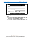
DMARQ
(device)
DMACK-
(host)
STOP
(host)
DDMARDY-
(device)
HSTROBE
(host)
DD(15:0)
(host)
DA0, DA1, DA2,
CS0-, CS1-
t
ACK
t
MLI
t
DVS
t
LI
t
LI
t
ACK
CRC
t
DVH
t
ACK
t
IORDYZ
t
MLI
t
RP
t
RFS