


ELECTRICAL SPECIFICATION SSD-DXXX(I)-4210 DATA SHEET
SILICONSYSTEMS PROPRIETARY
This document and the information contained within it is confidential and proprietary to SiliconSystems, Inc.
All unauthorized use and/or reproduction is prohibited.
4210D-03DSR PAGE 16 FEBRUARY 2, 2009
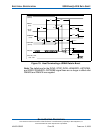
Note:
1. The symbol t
0
is the minimum total cycle time and t
D
is the minimum
command active time, while t
KR
and t
KW
are the minimum command
recovery times or command inactive times for input and output cycles,
respectively. The actual cycle time equals the sum of the actual command
active time and the actual command inactive time. The three timing
requirements of t
0
, t
D
, t
KR
, and t
KW
must be met. The minimum total cycle
time requirement is greater than the sum of t
D
and t
KR
, or t
KW
for input and
output cycles, respectively. This means a host implementation can lengthen
either or both of t
D
and either of t
KR
and t
KW
as needed to ensure that t
0
is
equal to or greater than the value reported in the device’s identify device
data.
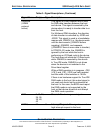
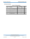
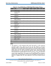
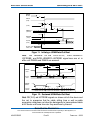
Table 12: True IDE Multiword DMA Read/Write Access Timing
Symbol Item Mode 0 Mode 1 Mode 2 Mode 3 Mode 4 Note Units
t
O
Cycle Time (minimum) 480 150 120 100 80 1 ns
t
D
-IORD/-IOWR
Asserted Width
(minimum)
215 80 70 65 55 1 ns
t
E
-IORD Data Access
(maximum)
150 60 50 50 45 - ns
t
F
-IORD Data Hold
(minimum)
5 5 5 5 5 - ns
t
G
-IORD/-IOWR Data
Setup (minimum)
100 30 20 15 10 - ns
t
H
-IOWR Data Hold
(minimum)
20 15 10 5 5 - ns
t
l
DMACK to –IORD/-
IOWR Setup
(minimum)
0 0 0 0 0 - ns
t
J
-IORD / -IOWR to -
DMACK Hold
(minimum)
20 5 5 5 5 - ns
t
KR
-IORD Negated Width
(minimum)
50 50 25 25 20 1 ns
t
KW
-IOWR Negated Width
(minimum)
215 50 25 25 20 1 ns
t
LR
-IORD to DMARQ
Delay (maximum)
120 40 35 35 35 - ns
t
LW
-IOWR to DMARQ
Delay (maximum)
40 40 35 35 35 - ns
t
M
CS(1:0) Valid to –
IORD / -IOWR
50 30 25 10 5 - ns
t
N
CS(1:0) Hold 15 10 10 10 10 - ns
t
Z
-DMACK 20 25 25 25 25 - ns