


ELECTRICAL SPECIFICATION SSD-DXXX(I)-4210 DATA SHEET
SILICONSYSTEMS PROPRIETARY
This document and the information contained within it is confidential and proprietary to SiliconSystems, Inc.
All unauthorized use and/or reproduction is prohibited.
4210D-03DSR PAGE 26 FEBRUARY 2, 2009
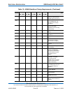
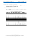
t
SS
50 - 50 - 50 - 50 - 50 - Time from STROBE edge to
negation of DMARQ or
assertion of STOP (when the
sender terminates a burst).
ns
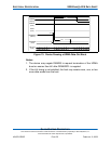
Notes:
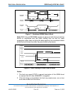
1. Timing parameters are measured at the connector of the sender or receiver to which the parameter applies.
Both STROBE and DMARDY- timing measurements are taken at the sender’s connector.
Example: For example, the sender stops generating STROBE edges t
RFS
after the negation of DMARDY-.
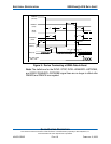
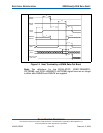
2. All timing measurement switching points (low-to-high and high-to-low) are taken at 1.5V.
3. The symbols t
UI
, t
MLI
, and t
LI
indicate sender-to-recipient or recipient-to-sender interlocks (i.e., either the sender
or recipient is waiting for the other to respond with a signal before proceeding). The symbol t
UI
is an unlimited
interlock that has no maximum time value, t
MLI
is a limited time-out that has a defined minimum, and t
LI
is a
limited time-out that has a defined maximum.
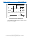
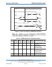
4. The test load for t
DVS
and t
DVH
are a lumped capacitor load with no cable or receivers. Timing for t
DVS
and t
DVH
are met for all capacitive loads from 15pF to 40pF where all signals have the same capacitive load value.
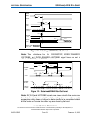
5. The symbol t
ZIORDY
may be greater than t
ENV
since the device has a pull-up on IORDY- giving it a known state
when released.
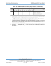
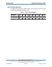
Table 13: UDMA Data Burst Timing Requirements (Continued)
Symbol
Mode 0 Mode 1 Mode 2 Mode 3 Mode 4
Comment (see Notes 1 and
2)
Units
Min. Max. Min. Max. Min. Max. Min. Max. Min. Max.