


Si53xx-RM
Rev. 0.5 105
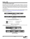
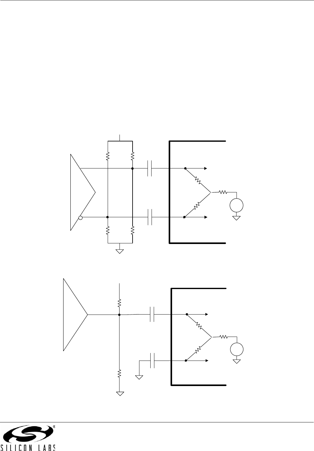
8. High-Speed I/O
8.1. Input Clock Buffers
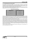
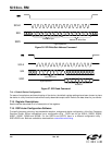
Any-Frequency Precision Clock devices provide differential inputs for the CKINn clock inputs. These inputs are
internally biased to a common mode voltage and can be driven by either a single-ended or differential source.
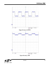
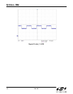
Figure 38 through Figure 41 show typical interface circuits for LVPECL, CML, LVDS, or CMOS input clocks. Note
that the jitter generation improves for higher levels on CKINn (within the limits in Table 8, “AC Characteristics—All
Devices”).
AC coupling the input clocks is recommended because it removes any issue with common mode input voltages.
However, either ac or dc coupling is acceptable. Figures 38 and 39 show various examples of different input
termination arrangements.
Unused inputs should have an AC ground connection. For microprocessor-controlled devices, the PD_CKn bits
may be set to shut off unused input buffers to reduce power.
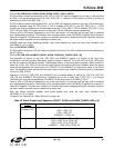
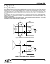
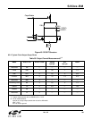
Figure 38. Differential LVPECL Termination
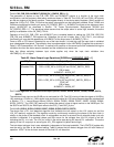
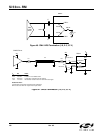
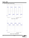
Figure 39. Single-Ended LVPECL Termination
40 k
C
C
±
CKIN
_
CKIN+
V
ICM
300
130
130
3.3 V
82
82
Si53xx
LVPECL
Driver
40 k
40 k
C
C
±
CKIN
_
CKIN +
V
ICM
300
130
3.3 V
82
Si53xx
Driver
40 k