


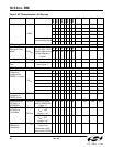
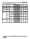
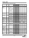
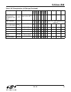
Si53xx-RM
36 Rev. 0.5
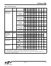
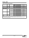
Input Mid Current I
IMM
See note
2
–2 — 2 µA
Input High Current I
IHH
See note
2
——20 µA
LVCMOS Output Pins
Output Voltage Low V
OL
I
O
=2mA
V
DD
=1.62V
——0.4 V
I
O
=2mA
V
DD
=2.97V
——0.4 V
Output Voltage High V
OH
I
O
=–2mA
V
DD
=1.62V
V
DD –
0.4
—— V
I
O
=–2mA
V
DD
=2.97V
V
DD –
0.4
—— V
Tri-State Leakage
Current
I
OZ
RST =0
–100 — 100 µA
Table 4. DC Characteristics (Continued)
Parameter Symbol Test Condition
Si5316
Si5322
Si5324
Si5325
Si5365
Si5366
Si5367
Si5368
Min Typ Max Units
Notes:
1. Refer to Section 6.7.1 and 8.2.1 for restrictions on output formats for TQFP devices at 3.3 V.
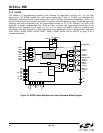
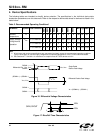
2. This is the amount of leakage that the 3L inputs can tolerate from an external driver. See Figure 55 on page 115.
3. No under- or overshoot is allowed.