


Si53xx-RM
Rev. 0.5 51
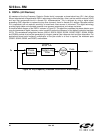
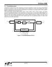
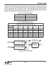
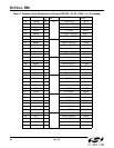
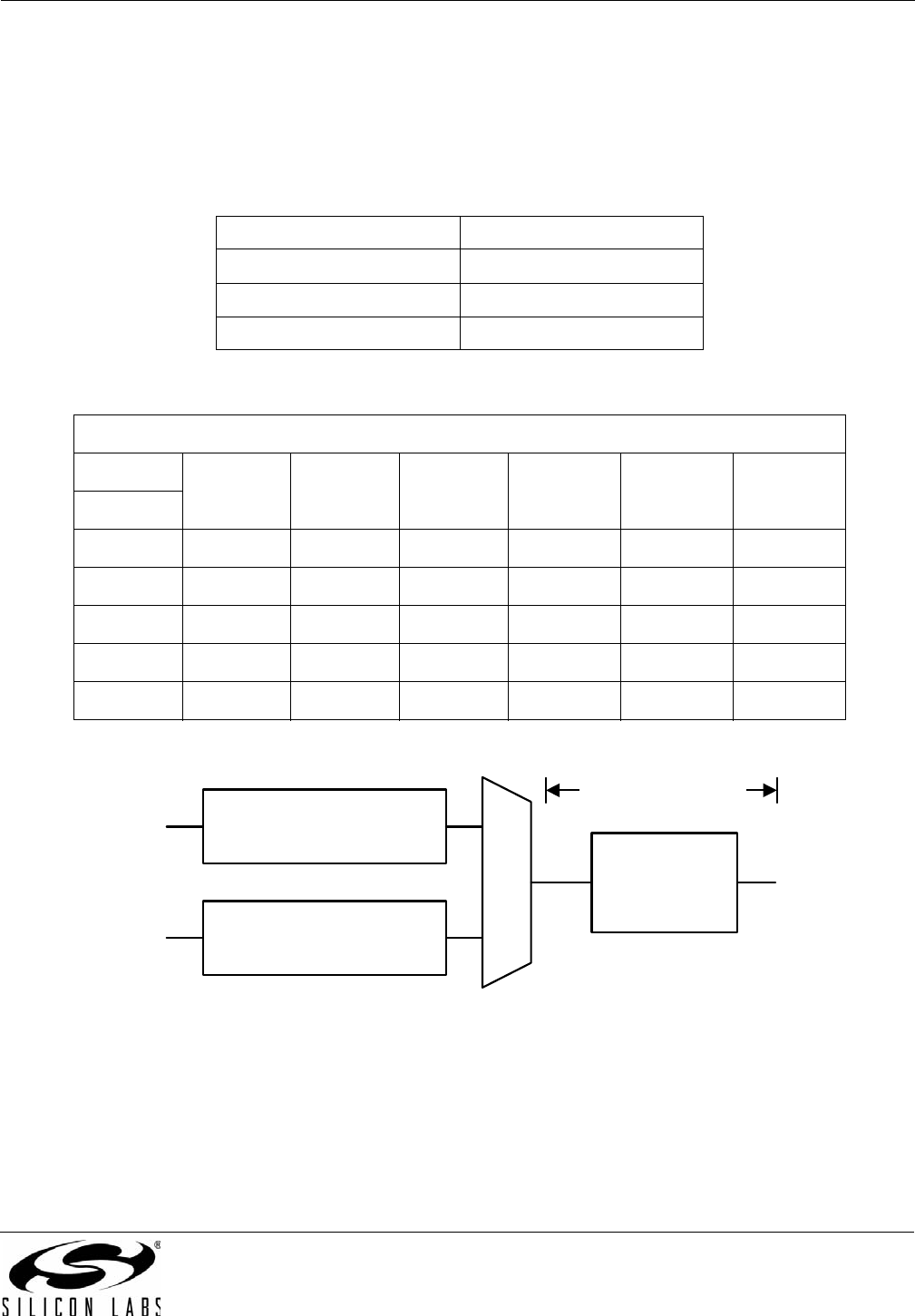
The Si5316 can accept a CKIN1 input at a different frequency than the CKIN2 input. The frequency of one input
clock can be 1x, 4x, or 32x the frequency of the other input clock. The output frequency is always equal to the lower
of the two clock inputs and is set via the FRQSEL [1:0] pins. The frequency applied at each clock input is divided
down by a pre-divider as shown in the Figure 1 on page 17. These pre-dividers must be set such that the two
resulting clock frequencies, f3_1 and f3_2 must be equal and are set by the FRQSEL [1:0] pins. Input divider
settings are controlled by the CK1DIV and CK2DIV pins, as shown in Table 14.
Figure 24. Si5316 Divisor Ratios
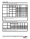
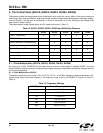
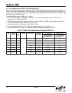
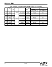
Table 14. Input Divider Settings
CKnDIV N3n Input Divider
L1
M4
H32
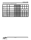
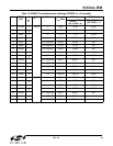
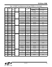
Table 15. Si5316 Bandwidth Values
FRQSEL[1:0] Nominal Frequency Values (MHz)
LL LM LH ML MM MH
BW[1:0] 19.44 MHz 38.88 MHz 77.76 MHz 155.52 MHz 311.04 MHz 622.08 MHz
HM 100 Hz 100 Hz 100 Hz 100 Hz 100 Hz 100 Hz
HL 210 Hz 210 Hz 200 Hz 200 Hz 200 Hz 200 Hz
MH 410 Hz 410 Hz 400 Hz 400 Hz 400 Hz 400 Hz
MM 1.7kHz 1.7kHz 1.6kHz 1.6kHz 1.6kHz 1.6kHz
ML 7.0kHz 7.0kHz 6.8kHz 6.7kHz 6.7kHz 6.7kHz
1, 4, 32
1, 4, 32
CKIN1
CKIN2
DSPLL
F
out
f
3
= F
out
f
3
One-to-one
frequency ratio