


Si53xx-RM
26 Rev. 0.5
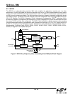
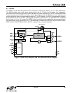
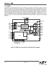
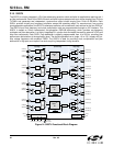
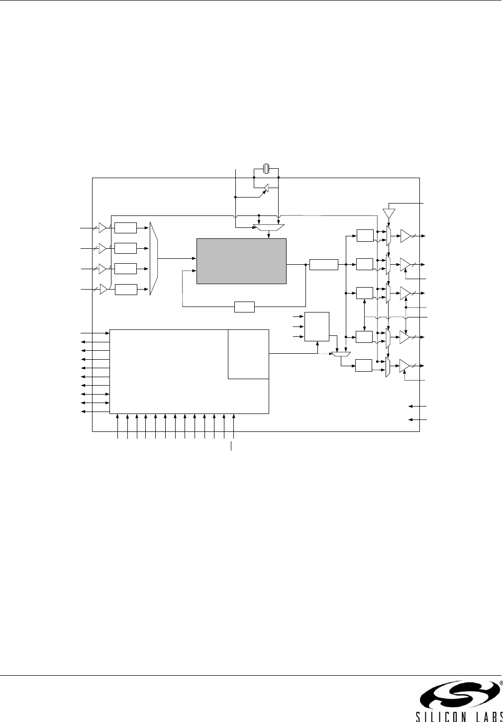
3.10. Si5366
The Si5366 is a jitter-attenuating precision clock multiplier for high-speed communication systems, including
SONET OC-48/OC-192, Ethernet, and Fibre Channel. The Si5366 accepts four clock inputs ranging from 8 kHz to
707 MHz and generates five frequency-multiplied clock outputs ranging from 8 kHz to 1050 MHz. The input clock
frequency and clock multiplication ratio are selectable from a table of popular SONET, Ethernet, Fibre Channel,
and broadcast video (HD SDI, 3G SDI) rates. The DSPLL loop bandwidth is digitally selectable from 60 Hz to
8 kHz, providing jitter performance optimization at the application level. Operating from a single 1.8, 2.5, or 3.3 V
supply, the Si5366 is ideal for providing clock multiplication and jitter attenuation in high performance timing
applications. See "6. Pin Control Parts (Si5316, Si5322, Si5323, Si5365, Si5366)" on page 50 for a complete
description.
Figure 10. Si5366 Jitter Attenuating Clock Multiplier Block Diagram
C2A
CS0_C3A
C2B
CS1_C4A
ALRMOUT
C1A
CKIN_1+
CKIN_1–
CKIN_2+
CKIN_2–
C3B
CKIN_3+
CKIN_3–
CKIN_4+
CKIN_4–
C1B
CKIN_3
CKIN_4
CKOUT_2
VDD
GND
CKOUT_1+
CKOUT_1–
÷ NC1
1
0
CKOUT_2+
CKOUT_2–
÷ NC2
1
0
CKOUT_3+
CKOUT_3–
÷ NC3
1
0
CKOUT_4+
CKOUT_4–
÷ NC4
1
0
2
2
2
2
2
2
2
2
f
OSC
Xtal or Refclock
RATE[1:0]
XA
XB
f
x
f
3
DBL2_BY
DBL34
DBL5
FSYNC
LOGIC/
ALIGN
CK_CONF
BWSEL[1:0]
FRQSEL[3:0]
DIV34[1:0]
FOS_CTL
SFOUT[1:0]
INC
DEC
FS_SW
FS_ALIGN
RST
CMODE
AUTOSEL
BYPASS/DSBL2
LOL
Control
÷ N3_2
÷ N3_1
FSYNC
3
÷ N3_3
÷ N3_4
CKOUT_5+
CKOUT_5–
÷ NC5
1
0
2
1
0
FRQTBL
DIV34[1:0]
÷ N1_HS
DSPLL
®
÷ N2