


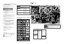
Note:
• All capacitors are in µF unless otherwise noted. (pF: µµF)
Capacitors without voltage indication are all 50 V.
• Indication of resistance, which does not have one for rating
electrical power, is as follows.
Pitch: 5 mm
Rating electrical power 1/4 W (CHIP : 1/10 W)
• All resistors are in ohms.
•
f : nonflammable resistor.
• Ï : fusible resistor.
•
f : internal component.
•
p : panel designation, and adjustment for repair.
• All variable and adjustable resistors have characteristic curve B,
unless otherwise noted.
•
e : earth-ground.
• E : earth-chassis.
• The components identified by
[ in this basic schematic diagram
have been carefully factory-selected for each set in order to
satisfy regulations regarding X-ray radiation.
Should replacement be required, replace only with the value
originally used.
• When replacing components identified by
], make the
necessary adjustments indicated. (See page 3-1)
• When replacing the part in below table, be sure to perform the
related adjustment.
5-7
5-8
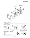
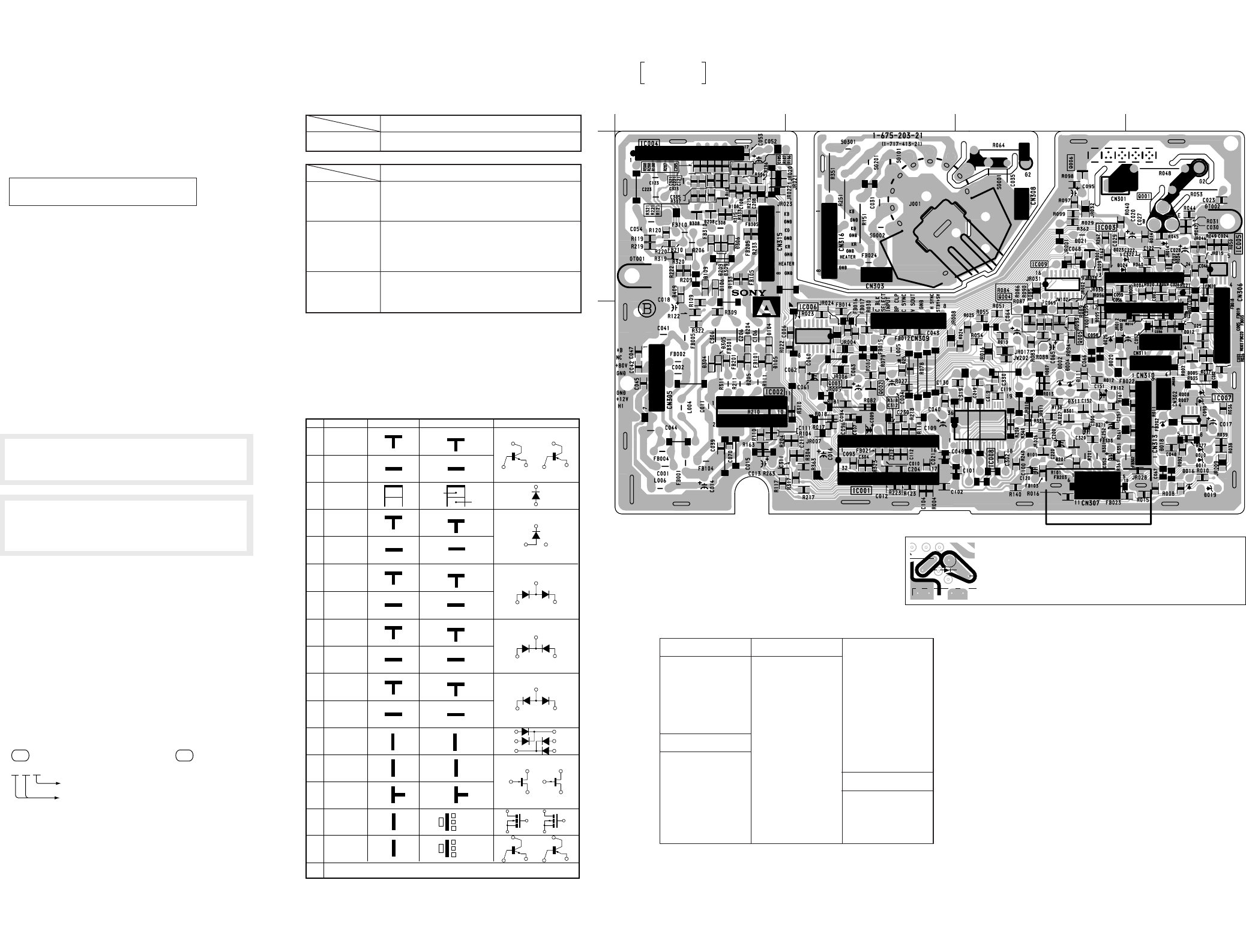
5-4. SCHEMATIC DIAGRAMS AND PRINTED
WIRING BOARDS
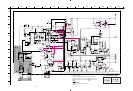
G
D
S
2
3
4
5
6
7
8
9
0
qa
qs
qf
qh
–
1
G
D
S
G
S
S
D
G
D
Ver.1.6
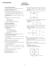
Transistor
(FET)
Transistor
Transistor
Discrete semiconductot
(Chip semiconductors that are not actually used are included.)
Diode
Diode
Diode
Diode
Diode
Diode
Diode
Diode
Diode
Diode
Source
Source
Anode
Anode
(NC)
(NC)
Cathode
Anode
Cathode
Common
Cathode
Cathode
Common
Cathode
Cathode
Common
Common
Common
Common
Cathode
Anode
Base
Emitter
Collector
Base
Emitter
Collector
Drain
Gate
Gate
Drain
Device Printed symbol Terminal name
Circuit
Terminal name of semiconductors in silk screen
printed circuit ( )
Anode
Anode
Anode Cathode
Anode Anode
Cathode
qd
Transistor
(FET)
Transistor
(FET)
qg
Emitter
Collector
Base
Transistor
Source
Gate
Drain
Cathode
Anode
Anode
Cathode
Anode
Anode
*
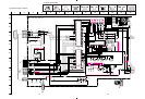
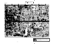
• Divided circuit diagram
One sheet of D board circuit diagram is divided into three sheets,
each having the code D-a to D-c. For example, the destination
ab1 on the code D-a sheet is connected to ab1 on the D-b sheet.
a b 1
Ref. No.
Circuit diagram division code
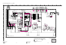
HV ADJ
Part Replaced ([)
RV901
HV Regulator
Circuit Check
HV Protector
Circuit Check
Beam Current
Protector Circuit
Check
Part Replaced (])
D Board T901 (FBT), IC901,
R924, R925, RV901
• Mounted D board
D Board T901 (FBT), R917, R918,
R923, R920, R919, R1004,
C920, D911, D912
• Mounted D board
D Board R933, R932, R921, R1006,
D915, D917, IC901, T901 (FBT)
• Mounted D board
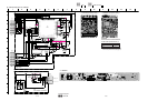
• All voltages are in V.
• Readings are taken with a 10 MΩ digital multimeter.
• Readings are taken with a color-bar signal input.
• Voltage variations may be noted due to normal production
tolerances.
•
*
: Can not be measured.
• Circled numbers are waveform references.
•
s : B + bus.
•
S : B – bus.
Note: The components identified by shading and
mark 0 are critical for safety. Replace only
with part number specified.
Note: Les composants identifiés per un tramé et
une marque 0 sont critiques pour la
sécurité. Ne les remplacer que par une pièce
portant le numéro spécifié.
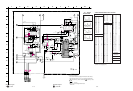
A
VIDEO AMP
RGB OUT
— A BOARD —
NOTE:
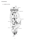
The circuit indicated as left contains high voltage of over
600 Vp-p. Care must be paid to prevent an electric shock in
inspection or repairing.
*
:Refer to Terminal name of semiconductors
in silk screen printed circuit (see page 5-7)
• A BOARD SEMICONDUCTOR LOCATION
IC
IC001 B-2
IC002 B-1
IC003 A-4
IC004 A-1
IC005 A-4
IC006 B-2
TRANSISTOR
*
Q001 A-4 –
Q002 B-2 1
Q003 B-2 1
Q006 A-3 1
DIODE
*
D002 B-3 –
D004 B-3 –
D005 B-4 6
D007 B-4 –
D008 B-4 –
D014 A-4 –
D023 A-3 –
D024 A-3 –
D025 B-3 –
D104 B-1 3
D105 B-1 3
D106 A-1 3
D108 A-1 6
D109 A-1 3
D111 B-3 6
D204 B-1 3
D205 B-1 3
D206 A-1 3
D208 A-1 6
D209 A-1 3
D211 B-3 6
D301 B-3 6
D304 B-1 3
D305 B-1 3
D306 A-1 3
D308 A-1 6
D309 A-1 3
D311 B-3 7
D409 A-1 3
CRYSTAL
X001 B-3
1 2 34
A
B