High Performance Two Port 10/100 Managed Ethernet Switch with 32-Bit Non-PCI CPU Interface
Datasheet
Revision 1.4 (08-19-08) 164 SMSC LAN9312
DATASHEET
GPIO_INT_POL[9:8] bits also determine the polarity of the clock events as described in
Section 13.2.1.2.
13.2.2.2 IEEE 1588 GPIO Interrupts
In addition to the standard GPIO interrupts in the General Purpose I/O Interrupt Status and Enable
Register (GPIO_INT_STS_EN), the IEEE 1588 timestamp enabled GPIO[9:8] pins contain the ability
to generate and clear specific IEEE 1588 related interrupts. When GPIO 9 or GPIO 8 are enabled as
inputs and an active edge occurs, the IEEE 1588 clock capture is indicated by the 1588_GPIO9_INT
and 1588_GPIO8_INT interrupts respectively in the 1588 Interrupt Status and Enable Register
(1588_INT_STS_EN). These interrupts are enabled by setting the corresponding 1588_GPIO9_EN
and 1588_GPIO8_EN bits in the 1588 Interrupt Status and Enable Register (1588_INT_STS_EN).
GPIO inputs must be active for greater than 40nS to be recognized as capture events.
When GPIO 8 and GPIO 9 are enabled, the 1588 Timer Interrupt bit (1588_TIMER_INT) of the 1588
Interrupt Status and Enable Register (1588_INT_STS_EN) can be cleared by an active edge on
GPIO[9:8]. A clear is only registered when the GPIO input is active for greater than 40nS.
13.3 LED Operation
Eight pins, GPIO[7:0], are shared with LED functions (nP1LED[3:0] and nP2LED[3:0]). These pins are
configured as LED outputs by setting the corresponding LED_EN bit in the LED Configuration Register
(LED_CFG). When configured as a LED, the pin is an open-drain, active-low output and the GPIO
related input buffer and pull-up are disabled. The LED outputs are always active low. As a result, a
low signal on the LED pin equates to the LED “on”, and a high signal equates to the LED “off”.
The functions associated with each LED pin are configurable via the LED_FUN[1:0] bits of the LED
Configuration Register (LED_CFG). These bits allow the configuration of each LED pin to indicate
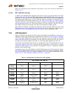
various port related functions. These functions are described in Table 13.1 followed by a detailed
definition of each indication type.
The default values of the LED_FUN[1:0] and LED_EN[7:0] bits of the LED Configuration Register
(LED_CFG) are determined by the LED_fun_strap[1:0] and LED_en_strap[7:0] configuration straps.
For more information on the LED Configuration Register (LED_CFG) and its related straps, refer to
Section 14.2.3.4, "LED Configuration Register (LED_CFG)," on page 196.
Table 13.1 LED Operation as a Function of LED_CFG[9:8]
LED_CFG[9:8] (LED_FUN[1:0])
00b 01b 10b 11b
nP2LED3
(GPIO7)
RX
Port 0
RX
Port 0
Activity
Port 2
-
nP2LED2
(GPIO6)
Link / Activity
Port 2
100Link / Activity
Port 2
Link
Port 2
-
nP2LED1
(GPIO5)
Full-duplex / Collision
Port 2
Full-duplex / Collision
Port 2
Full-duplex / Collision
Port 2
TXEN
Port 2
nP2LED0
(GPIO4)
Speed
Port 2
10Link / Activity
Port 2
Speed
Port 2
RXDV
Port 2
nP1LED3
(GPIO3)
TX
Port 0
TX
Port 0
Activity
Port 1
TXEN
Port 0
nP1LED2
(GPIO2)
Link / Activity
Port 1
100Link / Activity
Port 1
Link
Port 1
RXDV
Port 0


