


32 www.xilinx.com MicroBlaze Processor Reference Guide
1-800-255-7778 UG081 (v6.0) June 1, 2006
Chapter 1: MicroBlaze Architecture
R
Branches
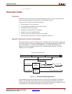
Normally the instructions in the fetch and decode stages (as well as prefetch buffer) are
flushed when executing a taken branch. The fetch pipeline stage is then reloaded with a
new instruction from the calculated branch address. A taken branch in MicroBlaze takes
three clock cycles to execute, two of which are required for refilling the pipeline. To reduce
this latency overhead, MicroBlaze supports branches with delay slots.
Delay Slots
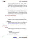
When executing a taken branch with delay slot, only the fetch pipeline stage in MicroBlaze
is flushed. The instruction in the decode stage (branch delay slot) is allowed to complete.
This technique effectively reduces the branch penalty from two clock cycles to one. Branch
instructions with delay slots have a D appended to the instruction mnemonic. For
example, the BNE instruction will not execute the subsequent instruction (does not have a
delay slot), whereas BNED will execute the next instruction before control is transferred to
the branch location.
A delay slot must not contain the following instructions: IMM, branch, or break. Interrupts
and external hardware breaks are deferred until after the delay slot branch has been
completed.
Instructions that could cause recoverable exceptions (e.g. unaligned word or halfword
load and store) are allowed in the delay slot. If an exception is caused in a delay slot the
ESR[DS] bit will be set, and the exception handler is responsible for returning the
execution to the branch target (stored in the special purpose register BTR) rather than the
sequential return address stored in R17.
Memory Architecture
MicroBlaze is implemented with a Harvard memory architecture, i.e. instruction and data
accesses are done in separate address spaces. Each address space has a 32 bit range (i.e.
handles up to 4 GByte of instructions and data memory respectively). The instruction and
data memory ranges can be made to overlap by mapping them both to the same physical
memory. The latter is useful e.g. for software debugging.
Both instruction and data interfaces of MicroBlaze are 32 bit wide and use big endian, bit-
reversed format. MicroBlaze supports word, halfword, and byte accesses to data memory.
Data accesses must be aligned (i.e. word accesses must be on word boundaries, halfword
on halfword bounders), unless the processor is configured to support unaligned
exceptions. All instruction accesses must be word aligned.
MicroBlaze does not separate between data accesses to I/O and memory (i.e. it uses
memory mapped I/O). Theprocessor has up to three interfaces for memory accesses: Local
Memory Bus (LMB), On-Chip Peripheral Bus (OPB), and Xilinx CacheLink (XCL). The
LMB memory address range must not overlap with OPB or XCL ranges.
MicroBlaze has a single cycle latency for accesses to local memory (LMB) and for cache
read hits. A data cache write normally has two cycles of latency (more if the posted-write
buffer in the memory controller is full).
For details on the different memory interfaces please refer to Chapter 2, “MicroBlaze
Signal Interface Description”.