


50 www.xilinx.com MicroBlaze Processor Reference Guide
1-800-255-7778 UG081 (v6.0) June 1, 2006
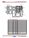
Chapter 2: MicroBlaze Signal Interface Description
R
Data_Write[0:31]
The write data bus is an output from the core and contains the data that is written to
memory. It becomes valid when AS is high and goes invalid in the clock cycle after Ready
is sampled high. Only the byte lanes specified by Byte_Enable[0:3] contain valid data.
AS
The address strobe is an output from the core and indicates the start of a transfer and
qualifies the address bus and the byte enables. It is high only in the first clock cycle of the
transfer, after which it goes low and remains low until the start of the next transfer.
Read_Strobe
The read strobe is an output from the core and indicates that a read transfer is in progress.
This signal goes high in the first clock cycle of the transfer, and remains high until the clock
cycle after Ready is sampled high. If a new read transfer is started in the clock cycle after
Ready is high, then Read_Strobe remains high.
Write_Strobe
The write strobe is an output from the core and indicates that a write transfer is in progress.
This signal goes high in the first clock cycle of the transfer, and remains high until the clock
cycle after Ready is sampled high. If a new write transfer is started in the clock cycle after
Ready is high, then Write_Strobe remains high.
Data_Read[0:31]
The read data bus is an input to the core and contains data read from memory.
Data_Read[0:31] is valid on the rising edge of the clock when Ready is high.
Ready
The Ready signal is an input to the core and indicates completion of the current transfer
and that the next transfer can begin in the following clock cycle. It is sampled on the rising
edge of the clock. For reads, this signal indicates the Data_Read[0:31] bus is valid, and for
writes it indicates that the Data_Write[0:31] bus has been written to local memory.
Clk
All operations on the LMB are synchronous to the MicroBlaze core clock.
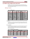
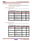
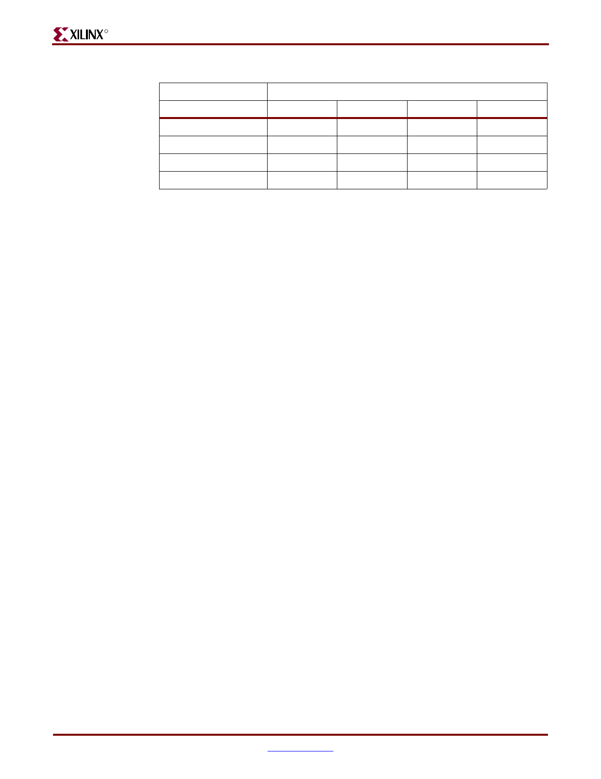
1000 x
0011 x x
1100 x x
1111 x x x x
Table 2-3: Valid Values for Byte_Enable[0:3]
Byte Lanes Used
Byte_Enable[0:3] Data[0:7] Data[8:15] Data[16:23] Data[24:31]