


ADSP-2186
–10–
REV. 0
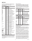
Bootstrap Loading (Booting)
The ADSP-2186 has two mechanisms to allow automatic load-
ing of the internal program memory after reset. The method for
booting is controlled by the Mode A, B and C configuration bits
as shown in Table VI. These four states can be compressed into
two-state bits by allowing an IDMA boot with Mode C = 1.
However, three bits are used to ensure future compatibility with
parts containing internal program memory ROM.
BDMA Booting
When the MODE pins specify BDMA booting, the ADSP-2186
initiates a BDMA boot sequence when RESET is released.
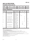
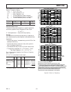
Table VI. Boot Summary Table
MODE C MODE B MODE A Booting Method
0 0 0 BDMA feature is used to load
the first 32 program memory
words from the byte memory
space. Program execution is
held off until all 32 words
have been loaded. Chip is
configured in Full Memory
Mode.
0 1 0 No Automatic boot opera-
tions occur. Program execu-
tion starts at external memory
location 0. Chip is config-
ured in Full Memory Mode.
BDMA can still be used but
the processor does not auto-
matically use or wait for these
operations.
1 0 0 BDMA feature is used to load
the first 32 program memory
words from the byte memory
space. Program execution is
held off until all 32 words
have been loaded. Chip is
configured in Host Mode.
Additional interface hardware
is required.
1 0 1 IDMA feature is used to load
any internal memory as de-
sired. Program execution is
held off until internal pro-
gram memory location 0 is
written to. Chip is configured
in Host Mode.
The BDMA interface is set up during reset to the following de-
faults when BDMA booting is specified: the BDIR, BMPAGE,
BIAD and BEAD registers are set to 0; the BTYPE register is
set to 0 to specify program memory 24 bit words; and the
BWCOUNT register is set to 32. This causes 32 words of on-
chip program memory to be loaded from byte memory. These
32 words are used to set up the BDMA to load in the remaining
program code. The BCR bit is also set to 1, which causes pro-
gram execution to be held off until all 32 words are loaded into
on-chip program memory. Execution then begins at address 0.
The ADSP-2100 Family development software (Revision 5.02
and later) fully supports the BDMA booting feature and can
generate byte memory space compatible boot code.
The IDLE instruction can also be used to allow the processor to
hold off execution while booting continues through the BDMA
interface. For BDMA accesses while in Host Mode, the ad-
dresses to boot memory must be constructed externally to the
ADSP-2186. The only memory address bit provided by the
processor is A0.
IDMA Port Booting
The ADSP-2186 can also boot programs through its Internal
DMA port. If Mode C = 1, Mode B = 0, and Mode A = 1, the
ADSP-2186 boots from the IDMA port. IDMA feature can load
as much on-chip memory as desired. Program execution is held
off until on-chip program memory location 0 is written to.
Bus Request & Bus Grant
The ADSP-2186 can relinquish control of the data and address
buses to an external device. When the external device requires
access to memory, it asserts the bus request (BR) signal. If the
ADSP-2186 is not performing an external memory access, it
responds to the active BR input in the following processor cycle
by:
• Three-stating the data and address buses and the PMS, DMS,
BMS, CMS, IOMS, RD, WR output drivers,
• Asserting the bus grant (BG) signal, and
• Halting program execution.
If Go Mode is enabled, the ADSP-2186 will not halt program
execution until it encounters an instruction that requires an
external memory access.
If the ADSP-2186 is performing an external memory access
when the external device asserts the BR signal, then it will not
three-state the memory interfaces or assert the BG signal until
the processor cycle after the access completes. The instruction
does not need to be completed when the bus is granted. If a
single instruction requires two external memory accesses, the
bus will be granted between the two accesses.
When the BR signal is released, the processor releases the BG
signal, reenables the output drivers and continues program
execution from the point where it stopped.
The bus request feature operates at all times, including when
the processor is booting and when RESET is active.
The BGH pin is asserted when the ADSP-2186 is ready to
execute an instruction but is stopped because the external bus is
already granted to another device. The other device can release
the bus by deasserting bus request. Once the bus is released, the
ADSP-2186 deasserts BG and BGH and executes the external
memory access.
Flag I/O Pins
The ADSP-2186 has eight general purpose programmable input/
output flag pins. They are controlled by two memory mapped
registers. The PFTYPE register determines the direction,
1 = output and 0 = input. The PFDATA register is used to read
and write the values on the pins. Data being read from a pin