


ADSP-2186
–16–
REV. 0
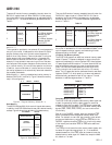
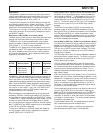
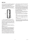
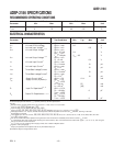
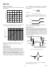
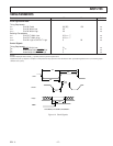
CAPACITIVE LOADING
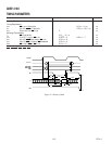
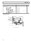
Figures 9 and 10 show the capacitive loading characteristics of
the ADSP-2186.
C
L
– pF
RISE TIME (0.4V–2.4V) – ns
30
3000
50
100 150 200 250
25
15
10
5
0
20
T = +85°C
V
DD
= 4.5V
Figure 9. Typical Output Rise Time vs. Load Capacitance,
C
L
(at Maximum Ambient Operating Temperature)
C
L
– pF
14
0
VALID OUTPUT DELAY OR HOLD – ns
50
100 150 250200
12
4
2
–2
10
8
NOMINAL
16
18
6
–4
–6
Figure 10. Typical Output Valid Delay or Hold vs. Load
Capacitance, C
L
(at Maximum Ambient Operating
Temperature)
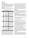
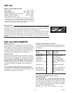
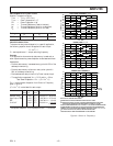
TEST CONDITIONS
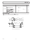
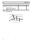
Output Disable Time
Output pins are considered to be disabled when they have
stopped driving and started a transition from the measured
output high or low voltage to a high impedance state. The out-
put disable time (t
DIS
) is the difference of t
MEASURED
and t
DECAY
,
as shown in the Output Enable/Disable diagram. The time is the
interval from when a reference signal reaches a high or low
voltage level to when the output voltages have changed by 0.5 V
from the measured output high or low voltage. The decay time,
t
DECAY
, is dependent on the capacitive load, C
L
, and the current
load, i
L
, on the output pin. It can be approximated by the fol-
lowing equation:
t
DECAY
=
C
L
× 0.5V
i
L
from which
t
DIS
= t
MEASURED
– t
DECAY
is calculated. If multiple pins (such as the data bus) are dis-
abled, the measurement value is that of the last pin to stop
driving.
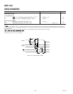
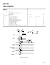
1.5V
2.0V
1.5V
0.8V
INPUT
OUTPUT
Figure 11. Voltage Reference Levels for AC Measure-
ments (Except Output Enable/Disable)
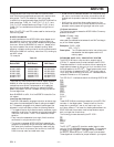
Output Enable Time
Output pins are considered to be enabled when that have made
a transition from a high-impedance state to when they start
driving. The output enable time (t
ENA
) is the interval from when
a reference signal reaches a high or low voltage level to when the
output has reached a specified high or low trip point, as shown
in the Output Enable/Disable diagram. If multiple pins (such as
the data bus) are enabled, the measurement value is that of the
first pin to start driving.
2.0V
1.0V
t
ENA
REFERENCE
SIGNAL
OUTPUT
t
DECAY
V
OH
(MEASURED)
OUTPUT STOPS
DRIVING
OUTPUT STARTS
DRIVING
t
DIS
t
MEASURED
V
OL
(MEASURED)
V
OH
(MEASURED) – 0.5V
V
OL
(MEASURED) +0.5V
HIGH-IMPEDANCE STATE. TEST CONDITIONS CAUSE
THIS VOLTAGE LEVEL TO BE APPROXIMATELY 1.5V.
V
OH
(MEASURED)
V
OL
(MEASURED)
Figure 12. Output Enable/Disable
TO
OUTPUT
PIN
50pF
+1.5V
I
OH
I
OL
Figure 13. Equivalent Device Loading for AC Measure-
ments (Including All Fixtures)