


ADSP-2186
–11–
REV. 0
configured as an input is synchronized to the ADSP-2186’s
clock. Bits that are programmed as outputs will read the value
being output. The PF pins default to input during reset.
In addition to the programmable flags, the ADSP-2186 has five
fixed-mode flags, FLAG_IN, FLAG_OUT, FL0, FL1 and
FL2. FL0-FL2 are dedicated output flags. FLAG_IN and
FLAG_OUT are available as an alternate configuration of
SPORT1.
Note: Pins PF0, PF1 and PF2 are also used for device configu-
ration during reset.
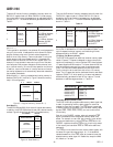
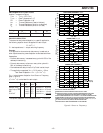
BIASED ROUNDING
A mode is available on the ADSP-2186 to allow biased round-
ing in addition to the normal unbiased rounding. When the
BIASRND bit is set to 0, the normal unbiased rounding opera-
tions occur. When the BIASRND bit is set to 1, biased round-
ing occurs instead of the normal unbiased rounding. When
operating in biased rounding mode all rounding operations with
MR0 set to 0x8000 will round up, rather than only rounding up
odd MR1 values.
For example:
Table VII.
MR Value Biased Unbiased
Before RND RND Result RND Result
00-0000-8000 00-0001-8000 00-0000-8000
00-0001-8000 00-0002-8000 00-0002-8000
00-0000-8001 00-0001-8001 00-0001-8001
00-0001-8001 00-0002-8001 00-0002-8001
00-0000-7FFF 00-0000-7FFF 00-0000-7FFF
00-0001-7FFF 00-0001-7FFF 00-0001-7FFF
This mode only has an effect when the MR0 register contains
0x8000; all other rounding operations work normally. This
mode allows more efficient implementation of bit-specified
algorithms that use biased rounding, for example the GSM
speech compression routines. Unbiased rounding is preferred
for most algorithms.
Note: BIASRND bit is Bit 12 of the SPORT0 Autobuffer Con-
trol register.
Instruction Set Description
The ADSP-2186 assembly language instruction set has an alge-
braic syntax that was designed for ease of coding and readabil-
ity. The assembly language, which takes full advantage of the
processor’s unique architecture, offers the following benefits:
• The algebraic syntax eliminates the need to remember cryptic
assembler mnemonics. For example, a typical arithmetic add
instruction, such as AR = AX0 + AY0, resembles a simple
equation.
• Every instruction assembles into a single, 24-bit word that
can execute in a single instruction cycle.
• The syntax is a superset ADSP-2100 Family assembly lan-
guage and is completely source and object code compatible
with other family members. Programs may need to be relo-
cated to utilize on-chip memory and conform to the ADSP-
2186’s interrupt vector and reset vector map.
• Sixteen condition codes are available. For conditional jump,
call, return or arithmetic instructions, the condition can be
checked and the operation executed in the same instruction
cycle.
• Multifunction instructions allow parallel execution of an
arithmetic instruction with up to two fetches or one write to
processor memory space during a single instruction cycle.
I/O Space Instructions
The instructions used to access the ADSP-2186’s I/O memory
space are as follows:
Syntax: IO(addr) = dreg
dreg = IO(addr);
where addr is an address value between 0 and 2047 and dreg is
any of the 16 data registers.
Examples: IO(23) = AR0;
AR1 = IO(17);
Description: The I/O space read and write instructions move
data between the data registers and the I/O
memory space.
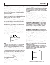
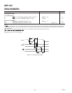
DESIGNING AN EZ-ICE
®
*-COMPATIBLE SYSTEM
The ADSP-2186 has on-chip emulation support and an
ICE-Port™*, a special set of pins that interface to the EZ-ICE
®
*.
These features allow in-circuit emulation without replacing the
target system processor by using only a 14-pin connection from
the target system to the EZ-ICE
®
*. Target systems must have a
14-pin connector to accept the EZ-ICE
®
*’s in-circuit probe, a
14-pin plug. See the ADSP-2100 Family EZ-Tools data sheet for
complete information on ICE products.
The ICE-Port™* interface consists of the following ADSP-2186
pins:
EBR
EBG
ERESET
EMS
EINT
ECLK
ELIN
ELOUT
EE
These ADSP-2186 pins must be connected only to the EZ-ICE
®
*
connector in the target system. These pins have no function
except during emulation, and do not require pull-up or
pull-down resistors. The traces for these signals between the
ADSP-2186 and the connector must be kept as short as pos-
sible, no longer than three inches.
The following pins are also used by the EZ-ICE
®
*:
BR
BG
RESET
GND
The EZ-ICE
®
* uses the EE (emulator enable) signal to take
control of the ADSP-2186 in the target system. This causes the
processor to use its ERESET, EBR and EBG pins instead of
the RESET, BR and BG pins. The BG output is three-stated.
These signals do not need to be jumper-isolated in your system.