


ADSP-2186
–4–
REV. 0
concurrently on multiplexed pins. In cases where pin func-
tionality is reconfigurable, the default state is shown in plain
text; alternate functionality is shown in italics.
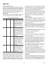
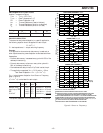
Common-Mode Pins
# Input/
Pin of Out-
Name(s) Pins put Function
RESET 1 I Processor Reset Input
BR 1 I Bus Request Input
BG 1 O Bus Grant Output
BGH 1 O Bus Grant Hung Output
DMS 1 O Data Memory Select Output
PMS 1 O Program Memory Select Output
IOMS 1 O Memory Select Output
BMS 1 O Byte Memory Select Output
CMS 1 O Combined Memory Select Output
RD 1 O Memory Read Enable Output
WR 1 O Memory Write Enable Output
IRQ2/ 1 I Edge- or Level-Sensitive
Interrupt Request
1
PF7 I/O Programmable I/O Pin
IRQL0/ 1 I Level-Sensitive Interrupt Requests
1
PF5 I/O Programmable I/O Pin
IRQL1/ 1 I Level-Sensitive Interrupt Requests
1
PF6 I/O Programmable I/O Pin
IRQE/ 1 I Edge-Sensitive Interrupt Requests
1
PF4 I/O Programmable I/O Pin
PF3 1 I/O Programmable I/O Pin
Mode C/ 1 I Mode Select Input—Checked
only During RESET
PF2 I/O Programmable I/O Pin During
Normal Operation
Mode B/ 1 I Mode Select Input—Checked
only During RESET
PF1 I/O Programmable I/O Pin During
Normal Operation
Mode A/ 1 I Mode Select Input—Checked
only During RESET
PF0 I/O Programmable I/O Pin During
Normal Operation
CLKIN, XTAL 2 I Clock or Quartz Crystal Input
CLKOUT 1 O Processor Clock Output
SPORT0 5 I/O Serial Port I/O Pins
SPORT1 5 I/O Serial Port I/O Pins
IRQ1:0 Edge- or Level-Sensitive Interrupts,
FI, FO Flag In, Flag Out
2
PWD 1 I Power-Down Control Input
PWDACK 1 O Power-Down Control Output
FL0, FL1, FL2 3 O Output Flags
V
DD
and GND 16 I Power and Ground
EZ-Port 9 I/O For Emulation Use
NOTES
1
Interrupt/Flag pins retain both functions concurrently. If IMASK is set to
enable the corresponding interrupts, the DSP will vector to the appropriate
interrupt vector address when the pin is asserted, either by external devices or
set as a programmable flag.
2
SPORT configuration determined by the DSP System Control Register. Soft-
ware configurable.
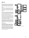
Memory Interface Pins
The ADSP-2186 processor can be used in one of two modes:
Full Memory Mode, which allows BDMA operation with full
external overlay memory and I/O capability, or Host Mode,
which allows IDMA operation with limited external addressing
capabilities. The operating mode is determined by the state of
the Mode C pin during RESET and cannot be changed while
the processor is running.
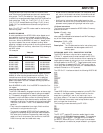
Full Memory Mode Pins (Mode C = 0)
#
of Input/
Pin Name Pins Output Function
A13:0 14 O Address Output Pins for Pro-
gram, Data, Byte and I/O Spaces
D23:0 24 I/O Data I/O Pins for Program,
Data, Byte and I/O Spaces
(8 MSBs Are Also Used as
Byte Memory Addresses)
Host Mode Pins (Mode C = 1)
#
of Input/
Pin Name Pins Output Function
IAD15:0 16 I/O IDMA Port Address/Data Bus
A0 1 O Address Pin for External I/O,
Program, Data, or Byte Access
D23:8 16 I/O Data I/O Pins for Program,
Data Byte and I/O Spaces
IWR 1 I IDMA Write Enable
IRD 1 I IDMA Read Enable
IAL 1 I IDMA Address Latch Pin
IS 1 I IDMA Select
IACK 1 O IDMA Port Acknowledge
In Host Mode, external peripheral addresses can be decoded using the A0,
CMS, PMS, DMS, and IOMS signals.
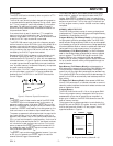
Setting Memory Mode
Memory Mode selection for the ADSP-2186 is made during
chip reset through the use of the Mode C pin. This pin is multi-
plexed with the DSP’s PF2 pin, so care must be taken in how
the mode selection is made. The two methods for selecting the
value of Mode C are active and passive.
Passive configuration involves the use a pull-up or pull-down
resistor connected to the Mode C pin. To minimize power
consumption, or if the PF2 pin is to be used as an output in the
DSP application, a weak pull-up or pull-down, on the order of
100 kΩ, can be used. This value should be sufficient to pull the
pin to the desired level and still allow the pin to operate as a
programmable flag output without undue strain on the processor’s
output driver. For minimum power consumption during
power-down, reconfigure PF2 to be an input, as the pull-up or
pull-down will hold the pin in a known state, and will not switch.
Active configuration involves the use of a three-stateable exter-
nal driver connected to the Mode C pin. A driver’s output en-
able should be connected to the DSP’s RESET signal such that
it only drives the PF2 pin when RESET is active (low). After
RESET is deasserted, the driver should three-state, thus allow-
ing full use of the PF2 pin as either an input or output.