


ADSP-2186
–6–
REV. 0
Idle
When the ADSP-2186 is in the Idle Mode, the processor waits
indefinitely in a low power state until an interrupt occurs. When
an unmasked interrupt occurs, it is serviced; execution then
continues with the instruction following the IDLE instruction.
In Idle mode IDMA, BDMA and autobuffer cycle steals still
occur.
Slow Idle
The IDLE instruction is enhanced on the ADSP-2186 to let the
processor’s internal clock signal be slowed, further reducing
power consumption. The reduced clock frequency, a program-
mable fraction of the normal clock rate, is specified by a select-
able divisor given in the IDLE instruction. The format of the
instruction is
IDLE (n);
where n = 16, 32, 64 or 128. This instruction keeps the proces-
sor fully functional, but operating at the slower clock rate. While
it is in this state, the processor’s other internal clock signals,
such as SCLK, CLKOUT and timer clock, are reduced by the
same ratio. The default form of the instruction, when no clock
divisor is given, is the standard IDLE instruction.
When the IDLE (n) instruction is used, it effectively slows down
the processor’s internal clock and thus its response time to in-
coming interrupts. The one-cycle response time of the standard
idle state is increased by n, the clock divisor. When an enabled
interrupt is received, the ADSP-2186 will remain in the idle
state for up to a maximum of n processor cycles (n = 16, 32, 64
or 128) before resuming normal operation.
When the IDLE (n) instruction is used in systems that have an
externally generated serial clock (SCLK), the serial clock rate
may be faster than the processor’s reduced internal clock rate.
Under these conditions, interrupts must not be generated at a
faster rate than can be serviced, due to the additional time the
processor takes to come out of the idle state (a maximum of n
processor cycles).
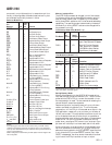
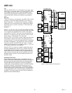
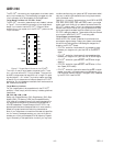
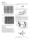
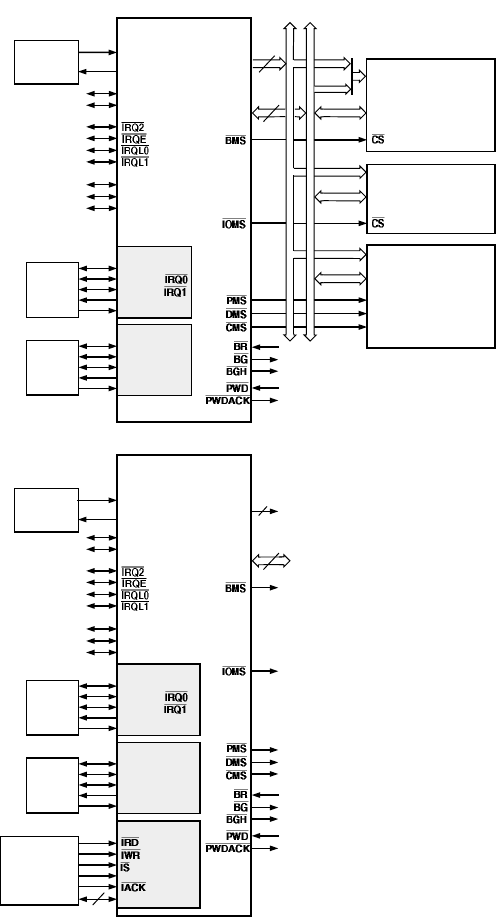
SYSTEM INTERFACE
Figure 2 shows typical basic system configurations with the
ADSP-2186, two serial devices, a byte-wide EPROM and optional
external program and data overlay memories (mode selectable).
Programmable wait state generation allows the processor to
connect easily to slow peripheral devices. The ADSP-2186 also
provides four external interrupts and two serial ports or six
external interrupts and one serial port. Host Memory Mode
allows access to the full external data bus, but limits addressing
to a single address bit (A0). Additional system peripherals can
be added in this mode through the use of external hardware to
generate and latch address signals.
1/2x CLOCK
OR
CRYSTAL
SERIAL
DEVICE
SERIAL
DEVICE
SCLK1
RFS1 OR
TFS1 OR
DT1 OR FO
DR1 OR FI
SPORT1
SCLK0
RFS0
TFS0
DT0
DR0
SPORT0
A0-A21
DATA
BYTE
MEMORY
I/O SPACE
(PERIPHERALS)
DATA
ADDR
DATA
ADDR
2048 LOCATIONS
OVERLAY
MEMORY
TWO 8K
PM SEGMENTS
TWO 8K
DM SEGMENTS
D
23-0
A
13-0
D
23-8
A
10-0
D
15-8
D
23-16
A
13-0
14
24
FL0-2
PF3
CLKIN
XTAL
ADDR13-0
DATA23-0
ADSP-2186
1/2x CLOCK
OR
CRYSTAL
SERIAL
DEVICE
SERIAL
DEVICE
SYSTEM
INTERFACE
OR
µCONTROLLER
16
1
16
SCLK1
RFS1 OR
TFS1 OR
DT1 OR FO
DR1 OR FI
SPORT1
SCLK0
RFS0
TFS0
DT0
DR0
SPORT0
/D6
/D7
/D4
IAL/D5
/D3
IAD15-0
IDMA PORT
FL0-2
PF3
CLKIN
XTAL
ADDR0
DATA23-8
ADSP-2186
/PF7
/PF4
/PF5
/PF6
MODE C/PF2
MODE B/PF1
MODE A/PF0
HOST MEMORY MODE
/PF7
/PF4
/PF5
/PF6
MODE C/PF2
MODE B/PF1
MODE A/PF0
FULL MEMORY MODE
Figure 2. Basic System Configuration