


ADSP-2186
–15–
REV. 0
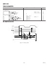
ENVIRONMENTAL CONDITIONS
Ambient Temperature Rating:
T
AMB
=T
CASE
– (PD x θ
CA
)
T
CASE
= Case Temperature in °C
PD = Power Dissipation in W
θ
CA
= Thermal Resistance (Case-to-Ambient)
θ
JA
= Thermal Resistance (Junction-to-Ambient)
θ
JC
= Thermal Resistance (Junction-to-Case)
Package
JA
JC
CA
TQFP 50°C/W 2°C/W 48°C/W
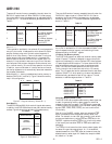
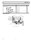
POWER DISSIPATION
To determine total power dissipation in a specific application,
the following equation should be applied for each output:
C × V
DD
2
× f
C = load capacitance, f = output switching frequency.
Example
In an application where external data memory is used and no
other outputs are active, power dissipation is calculated as follows:
Assumptions
• External data memory is accessed every cycle with 50% of the
address pins switching.
• External data memory writes occur every other cycle with
50% of the data pins switching.
• Each address and data pin has a 10 pF total load at the pin.
• The application operates at V
DD
= 5.0 V and t
CK
= 30 ns.
Total Power Dissipation = P
INT
+ (C × V
DD
2
× f)
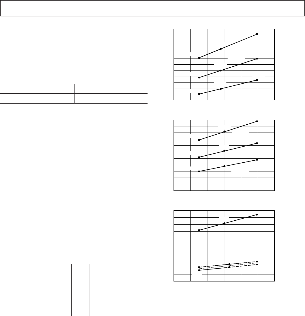
P
INT
= internal power dissipation from Power vs. Frequency
graph (Figure 8).
(C × V
DD
2
× f) is calculated for each output:
# of
Pins ؋ C ؋ V
DD
2
؋f
Address, DMS 8 × 10 pF × 5
2
V × 33.3 MHz = 66.6 mW
Data Output, WR 9 × 10 pF × 5
2
V × 16.67 MHz = 37.5 mW
RD 1 × 10 pF × 5
2
V × 16.67 MHz = 4.2 mW
CLKOUT 1 × 10 pF × 5
2
V × 33.3 MHz = 8.3 mW
116.6 mW
Total power dissipation for this example is PINT + 116.6 mW.
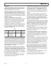
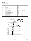
VALID FOR ALL TEMPERATURE GRADES.
1
POWER REFLECTS DEVICE OPERATING WITH NO OUTPUT LOADS.
5
SPECIFICATIONS AT 40MHz ARE PRELIMINARY AT THIS PRINTING.
4
I
DD
MEASUREMENT TAKEN WITH ALL INSTRUCTIONS EXECUTING FROM INTERNAL
MEMORY. 50% OF THE INSTRUCTIONS ARE MULTIFUNCTION (TYPES 1, 4, 5, 12, 13, 14
30% ARE TYPE 2 AND TYPE 6, AND 20% ARE IDLE INSTRUCTIONS.
3
TYPICAL POWER DISSIPATION AT 5.0V V
DD
AND T
A
= 25°C EXCEPT WHERE SPECIFIED.
2
IDLE REFERS TO ADSP-2186 STATE OF OPERATION DURING EXECUTION OF IDLE
INSTRUCTION. DEASSERTED PINS ARE DRIVEN TO EITHER V
DD
OR GND.
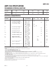
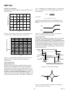
70
20
65
40
35
30
25
60
55
45
50
POWER (P
IDLE
n
) – mW
1/f
CK
– MHz
28 4230 32 34 36 38 40
56mW
30mW
28mW
32mW
30mW
34mW
32mW
61mW
67mW
IDLE (16)
IDLE (128)
IDLE
85
30
80
55
50
45
40
75
70
60
65
35
POWER (P
IDLE
) – mW
1/f
CK
– MHz
4230 32 34 36 38 40
69mW
76mW
84mW
V
DD
= 5.5V
56mW
61mW
67mW
V
DD
= 5.0V
45mW
49mW
54mW
V
DD
= 4.5V
1/f
CK
– MHz
4230 32 34 36 38 40
450
200
425
300
275
250
225
400
375
325
350
POWER (P
INT
) – mW
175
150
330mW
245mW
175mW
275mW
195mW
325mW
235mW
370mW
V
DD
= 5.5V
V
DD
= 5.0V
V
DD
= 4.5V
2186 POWER, INTERNAL
1, 3, 4, 5
POWER, IDLE
1, 2, 3, 5
POWER, IDLE
n
MODES
3, 5
430mW
Figure 8. Power vs. Frequency