


ADSP-2186
–5–
REV. 0
To minimize power consumption during power-down, configure
the programmable flag as an output when connected to a three-
stated buffer. This ensures that the pin will be held at a constant
level and not oscillate should the three-state driver’s level hover
around the logic switching point.
Interrupts
The interrupt controller allows the processor to respond to the
eleven possible interrupts and reset with minimum overhead.
The ADSP-2186 provides four dedicated external interrupt
input pins, IRQ2, IRQL0, IRQL1 and IRQE (shared with the
PF7:4 pins). In addition, SPORT1 may be reconfigured for
IRQ0, IRQ1, FLAG_IN and FLAG_OUT, for a total of six
external interrupts. The ADSP-2186 also supports internal
interrupts from the timer, the byte DMA port, the two serial
ports, software and the power-down control circuit. The inter-
rupt levels are internally prioritized and individually maskable
(except power-down and reset). The IRQ2, IRQ0 and IRQ1
input pins can be programmed to be either level- or edge-sensitive.
IRQL0 and IRQL1 are level-sensitive and IRQE is edge-sensitive.
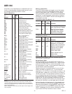
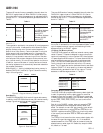
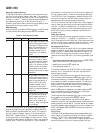
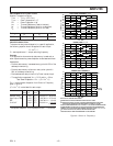
The priorities and vector addresses of all interrupts are shown in
Table I.
Table I. Interrupt Priority & Interrupt Vector Addresses
Source Of Interrupt Interrupt Vector Address (Hex)
Reset (or Power-Up with
PUCR = 1) 0000 (Highest Priority)
Power-Down (Nonmaskable) 002C
IRQ2 0004
IRQL1 0008
IRQL0 000C
SPORT0 Transmit 0010
SPORT0 Receive 0014
IRQE 0018
BDMA Interrupt 001C
SPORT1 Transmit or IRQ1 0020
SPORT1 Receive or IRQ0 0024
Timer 0028 (Lowest Priority)
Interrupt routines can either be nested, with higher priority
interrupts taking precedence, or processed sequentially. Inter-
rupts can be masked or unmasked with the IMASK register.
Individual interrupt requests are logically ANDed with the bits
in IMASK; the highest priority unmasked interrupt is then
selected. The power-down interrupt is nonmaskable.
The ADSP-2186 masks all interrupts for one instruction cycle
following the execution of an instruction that modifies the
IMASK register. This does not affect serial port autobuffering
or DMA transfers.
The interrupt control register, ICNTL, controls interrupt nest-
ing and defines the IRQ0, IRQ1 and IRQ2 external interrupts to
be either edge- or level-sensitive. The IRQE pin is an external
edge-sensitive interrupt and can be forced and cleared. The
IRQL0 and IRQL1 pins are external level-sensitive interrupts.
The IFC register is a write-only register used to force and clear
interrupts.
On-chip stacks preserve the processor status and are automati-
cally maintained during interrupt handling. The stacks are twelve
levels deep to allow interrupt, loop and subroutine nesting.
The following instructions allow global enable or disable servic-
ing of the interrupts (including power-down), regardless of the
state of IMASK. Disabling the interrupts does not affect serial
port autobuffering or DMA.
ENA INTS;
DIS INTS;
When the processor is reset, interrupt servicing is enabled.
LOW POWER OPERATION
The ADSP-2186 has three low power modes that significantly
reduce the power dissipation when the device operates under
standby conditions. These modes are:
• Power-Down
• Idle
• Slow Idle
The CLKOUT pin may also be disabled to reduce external
power dissipation.
Power-Down
The ADSP-2186 processor has a low power feature that lets the
processor enter a very low power dormant state through hard-
ware or software control. Here is a brief list of power-down
features. Refer to the ADSP-2100 Family User’s Manual, “System
Interface” chapter, for detailed information about the power-
down feature.
• Quick recovery from power-down. The processor begins
executing instructions in as few as 100 CLKIN cycles.
• Support for an externally generated TTL or CMOS proces-
sor clock. The external clock can continue running during
power-down without affecting the lowest power rating and
100 CLKIN cycle recovery.
• Support for crystal operation includes disabling the oscillator
to save power (the processor automatically waits approxi-
mately 4096 CLKIN cycles for the crystal oscillator to start
or stabilize), and letting the oscillator run to allow 100 CLKIN
cycle start-up.
• Power-down is initiated by either the power-down pin (PWD)
or the software power-down force bit.
• Interrupt support allows an unlimited number of instructions
to be executed before optionally powering down. The power-
down interrupt also can be used as a nonmaskable, edge-
sensitive interrupt.
• Context clear/save control allows the processor to continue
where it left off or start with a clean context when leaving the
power-down state.
• The RESET pin also can be used to terminate power-down.
• Power-down acknowledge pin indicates when the processor
has entered power-down.