


Circuit Description
4-2 AT91EB42 Evaluation Board User Guide
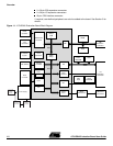
4.3 Memories The schematic (Figure 6-3 on page 6-4 in Section 6, “Appendix B – Schematics”) shows
one AT49BV1604 2 MB 16-bit Flash, one AT45DB321 4 MB serial DataFlash, one
AT24C512 64 KB EEPROM, one AT25256 32 KB EEPROM and two 128K/512K x 8
SRAM devices.
Note: The AT91EB42 is fitted with two 128K x 8 SRAM devices.
A footprint is provided for the user to fit a multi-chip device memory that embeds Flash
(1 MB) and SRAM (128 KB) in a single component in place of the Flash and SRAM
devices (U7: M36W108AB from ST).
Strap JP1 shown on the schematic is used to select the part of 1 MB of the Flash to be
accessed. This is to enable users to Flash download their application in the second part
of the Flash and to boot on it.
4.4 Analog-to-digital
Converter
A footprint is provided for the user to fit a 4-channel 10-bit ADC device (AD7817ARU
from Analog Devices; see Figure 6-10 on page 6-11 in Section 6, “Appendix B – Sche-
matics”). This device is interfaced to the AT91 microcontroller via the SPIA peripheral.
The voltage reference used is the 2.5V on-chip.
This device embeds a temperature sensor and is placed near the 32.768 KHz crystal
quartz. Thus the user is able to take into account the frequency drift due to temperature
evolution by a software program.
By default, two of the ADC channels are dedicated to supervise the board power supply
voltage levels (channel 1 for the battery power supply, channel 2 for the standard power
supply).
4.5 Power and
Crystal Quartz
The AT91M42800 master clock is derived from a 32.768 KHz crystal quartz. The on-
chip low-power oscillator together with two PLL-based frequency multipliers and the
prescaler results in a programmable master clock between 500 Hz and 33 MHz.
Two sets of components for the PLL filters are fitted by default on the board (Figure 6-6
on page 6-7 in Section 6, "Appendix B - Schematics"). They are calculated to provide a
16.77 MHz (PLLA: multiplier factor of 512 and settling time of 600
=µs) or a 33.55 MHz
(PLLB: multiplier factor of 1024 and settling time of 4 ms) master clock frequency.
The voltage regulator provides 3.3V to the board and will light the red POWER LED
(D11) when operating.
Power can be applied via the 2.1 mm connector to the regulator in either polarity
because of the diode-rectifying circuit. Another regulator allows the user to power the
AT91M42800 core with 3.3V or 1.8V by means of the JP8 jumper.
A battery power supply can be applied via the J3 connector. The type of battery and
connections to be used are shown in the schematics (Figure 6-9 on page 6-10 in Sec-
tion 6, "Appendix B - Schematics"). This type of battery will ensure the power supply of
the board for approximately 30 minutes. A battery fast-charge controller is provided on-
board to charge this battery. The number of series cells to be charged is set to 5, but
can be changed via the CB21, CB22 and CB32 configuration straps. The maximum time
allowed for fast-charging is set to 264 minutes.
4.6 Push Buttons,
LEDs, Reset and
Serial Interfaces
The IRQ0, TIOA0, PB6 and PB21 switches are debounced and buffered.
A supervisory circuit has been included in the design to detect and consequently reset
the board when the 3.3V supply voltage drops below 3.0V. Note that this voltage can be
changed depending on the board production series. The supervisory circuit also pro-
vides a debounced reset signal. This device can also generate the reset signal in case