


Circuit Description
AT91EB42 Evaluation Board User Guide 4-3
of watchdog time-out as the pin NWDOVF of the AT91M42800 is connected to its input
MR
.
The assertion of this reset signal will light up the red RESET LED (D10). By pressing the
CLEAR RESET push button (S1), the LED can be turned off.
Another supervisory circuit initializes separately the microcontroller-embedded
JTAG/ICE interface when the 3.3V supply voltage drops below 3.0V. Note that this volt-
age can be changed, depending on the board production series. These separated reset
lines allow the user to reset the board without resetting the JTAG/ICE interface while
debugging.
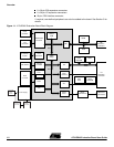
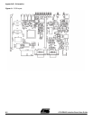
The schematic (Figure 6-5 on page 6-6 in Section 6, "Appendix B - Schematics") also
shows eight general-purpose LEDs connected to port B PIO pins (PB8 to PB15).
Two 9-way D-type connectors (P3/4) are provided for serial port connection.
Serial port A (P3) is used primarily for host PC communication and is a DB9 female con-
nector. TXD and RXD are swapped so that a straight-through cable can be used. CTS
and RTS are connected together, as are DCD, DSR and DTR.
Serial port B (P4) is a DB9 male connector with TXD and RXD obeying the standard
RS-232 pinout. Apart from TXD, RXD and ground, the other pins are not connected.
LEDs are connected to the TX and RX signals of both serial ports and show activity on
these serial links.
A MAX3223 device (U10) and associated bulk storage capacitors provide RS-232 level
conversion.
4.7 Layout Drawing The layout diagram (Figure 6-1 on page 6-2 in Section 6, “Appendix B – Schematics”)
shows an approximate floorplan for the board. This has been designed to give the low-
est board area, while still providing access to all test points, jumpers and switches on
the board.
The board is provided with four mounting holes, one at each corner, into which feet are
attached. The board has two signal layers and two power planes.