


Ref.:
UoD_SpW-10X_
UserManual
Issue:
3.4
SpW-10X
SpaceWire Router
User Manual
Date:
11
th
July 2008
Preliminary
140
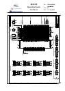
12.2 PCB DESIGN AND LAYOUT GUIDELINES
PCB design and layout guide lines are provided in this section.
12.2.1 CLK
1. Series termination should be used on the CLK signal.
2. Stubs on the CLK signal shall not be used.
3. Guard tracks shall be provided around the CLK signal trace connected to the ground plane
approximately every 1 cm.
12.2.2 RST_N
Guard tracks shall be provided around the RST_N signal trace connected to the ground plane
approximately every 1 cm.
12.2.3 Chip Test Signals
The two chip test signals TestIOEn and TestEn shall both be tied directly to the ground plane.
12.2.4 Power and Decoupling
1. Each power pin shall be decoupled to ground using a 100 nF decoupling capacitor.
2. The 100 nF decoupling capacitors shall be fitted close to the each power pin with the other
end of the capacitor connected to the ground plane.
3. In addition to the 100 nF decoupling capacitors four 1 µF decoupling capacitors shall be fitted
close to the SpW-10X device.
12.2.5 Ground
1. A solid ground plane shall be used.
2. The ground pins of the SpW-10X shall be directly connected to the ground plane using vias
close to the SpW-10X ground pins.
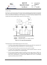
12.2.6 SpaceWire
The following recommendations apply to all the SpaceWire signals from the SpW-10X device (see
also section 5.2):
1. LVDS receiver termination resistor shall be as close as possible to the receiver inputs.