


Ref.:
UoD_SpW-10X_
UserManual
Issue:
3.4
SpW-10X
SpaceWire Router
User Manual
Date:
11
th
July 2008
Preliminary
142
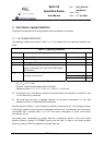
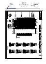
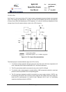
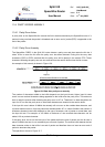
12.2.10 PLL
See Figure 12-1 the internal wiring of PLL block to better understand the external board recommended
layout. The Voltage drop between PLL loop filter (LF) and the PVCOBIAS pads will be converted into
a current (Ivco) which will determine the VCO frequency. It is critical to avoid any disturbance of that
voltage drop at this will translate directly to jitter in the VCO frequency.
Figure 12-1 PLL Layout Recommendations
The following layout recommendations apply to the PLL circuitry.
1. To minimize voltage parasitic through ground the loop filter and VCO bias components will
have a separate ground plane underneath all PLL pins and components.
2. This PLL ground plane shall be connected at one point to the PLLVSS pad.
3. To minimize other electromagnetic crosstalk effects, SMD components should be used and
placed as close as possible to the corresponding pads.
4. The PLL has been designed to exhibit low sensitivity to power supply variation. VDDPLL can
be externally connected to the core array power supply but the cleaner that power supply the
better the PLL performances is in terms of jitter. Separate 100 nF and 1 µF decoupling
capacitors shall be provided for VDDPLL.