


485SDA103798 Manual Appendix B B-1
B&B Electronics -- 707 Dayton Rd. -- PO Box 1040 -- Ottawa, IL 61350
PH (815) 433-5100 -- FAX (815) 434-7094
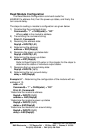
Appendix B: Analog Input Impedance
When interfacing with an A/D converter, it is important that the
device you are connecting can drive the A/D input. To determine if
your device can drive an A/D input, there are three factors you must
consider:
• Output impedance of the device
• Input impedance of A/D
• A/D sampling time
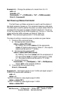
The goal is to have the voltage at the A/D input settle to a voltage
close to the output voltage of the device in a time frame that is less
than the A/D sampling time. (Close to means a value significantly
less than the resolution of the A/D). If the voltage does not settle
fast enough, errors will occur in the reading, resulting in a loss of
resolution.
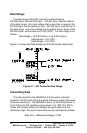
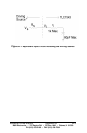
The next section, titled “Simplified Analog Input Analysis,”
contains information from Texas Instruments data sheet on the
TLC1543. The TLC1543 is the A/D converter that is used on the
485SDA10. This section provides a simplified calculation which can
be used to determine the maximum output impedance the device
can have to settle the A/D input to a voltage within one half LSB.
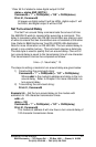
For the 485SDA10:
t us
c
=
100
Using this information:
R k
s
≤
170
Ω
If the output impedance of your device is 170kΩ, you should figure
an additional error of ½ LSB.
It should be pointed out that this is a simplified analysis and
there other several other factors that must be considered (pin
capacitance, noise immunity, etc.). The data sheet for the TLC1543
states that “The driving source impedance should be less than or
equal to 1kΩ.” B&B Electronics recommends placing a voltage
follower between the 485SDA10 and any device with output source
impedance greater than 1kΩ.