


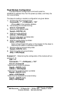

B-2 Appendix B 485SDA103798 Manual
B&B Electronics -- 707 Dayton Rd. -- PO Box 1040 -- Ottawa, IL 61350
PH (815) 433-5100 -- FAX (815) 434-7094
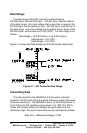
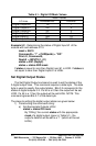
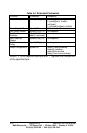
Simplified Analog Input Analysis
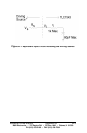
Using the equivalent circuit in Figure B-1, the time required to
charge the analog input capacitance from 0 to Vs within ½ LSB can
be derived as follows:
The capacitance charging voltage is given by
V V
t R C
e
c s
c t i
= −
−
( )1 (1)
where
R R r
t s i
=
+
The final voltage to ½ LSB is given by
V LSB V V
c s s
( ) ( )1 2 2048
=
−
(2)
Equating equation 1 to equation 2 and solving for time t
c
gives
V V V e
t R C
s s s
c t i
− = −
−
( ) ( )2048 1 (3)
and
t LSB R C
c t i
( ) ln( )1 2 2048
=
×
×
(4)
Therefore, with the values given the time for the analog input signal
to settle is
t LSB R
c s
( ) ( ) ln( )1 2 1 60 2048
=
+
×
×
k pF
Ω
(5)
This time must be less than the converter sample time shown in the
timing diagrams.
V
I
= Input Voltage at A0 - A10
V
S
= External Driving Source Voltage
R
S
= Source Resistance
r
i
= Input Resistance
C
i
= Equivalent Input Capacitance
*Driving source requirements:
• Noise and distortion for the source must be
equivalent to the resolution of the converter.
• R
S
must be real at the input frequency.