


Connect Tech Blue Heat/Net Sync User Manual
Revision 0.01 55
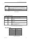
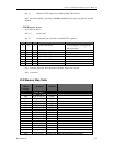
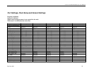
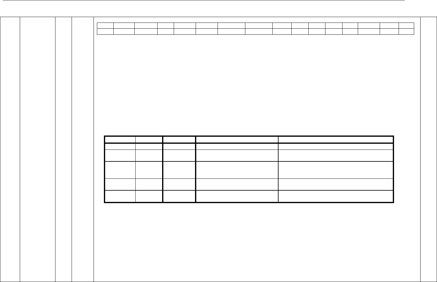
1008
100C
1010
1014
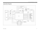
LIFC1,2,3,4
Line Interface
Control
1008= Port 1
100C = Port 2
1010 = Port 3
1014 = Port 4
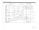
R/W
D15..0
Control Bits: Read/Write only as a 16 Bit word.
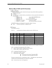
15
14
13
12
11
10
9
8
7
6
5
4
3
2
1
0
X
DCDC
DCDS
ES
FSM
CTSC
CTSM1
CTSM0
RTS
DC
42W
DM
SPT
SP2
SP1
SP0
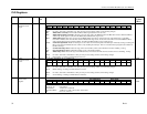
Important Note: These control bits are transferred to ALL the Line Interface PLD‟s by a serial interface. On each write to any of the 4 control registers, a serial
transfer is started. The transfer takes about 16uS to complete. During this time NO write can occur to any of the 4 registers. A Busy signal is available to indicated
that the transfer is in progress. (See the PLD_STATUS Register, below).
Basic Line Mode Control bits:
SP[2..0] SP508 Line Mode setting bits: See information in SP508 Data sheet. Power-up state=[111].
SPT SP508 Terminator Enable: 0=disable terminator, 1=enable terminator
Duplex Control and RTS Pin Control bits:
DM Duplex Mode selection: 0=Full, 1=Duplex.
42W 4/2 Wire mode selection: 0=2wire (or ½ Duplex), 1=4wire (or Multi-Drop Slave).
DC Duplex Control Source: 0=RTS signal from IUSC, 1=TXComplete signal from IUSC.
RTS RTS Pin Source Selection: 0=RTS signal from IUSC, 1=TXComplete signal from IUSC.
Notes: When Full Duplex mode is selected the “42W” and “DC” bits settings can be changed but are ignored.
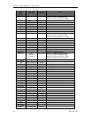
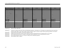
Triggered/Gated Transmission Control Bits
CTSM and FSM
FSM
CTSM[1]
CTSM[0]
FSYNC# pin on IUSC
CTS# pin on IUSC
X
0
0
---
Driven from Line Interface CTS signal
0
X
X
Driven directly from Trigger input
signal (inverted)
---
0
0
1
---
CTS pulsed low for 15 clock cycles [1] as follows…
If CTSC=0: clocked by Transmitter clock.
If CTSC=1: clocked by PLD clock (14.66 MHz)
1
0
1
FSYNC Pulsed for 5 or 1 Transmitter
clock cycles [1][2]
CTS pulsed low for 5 or 1 Transmitter clock cycles
[1][2]
X
1
0
---
CTS is turned ON when appropriate TRG bit is ON
(see TRG bits in the PLD_CNTRL register, below)
[1] Whenever the appropriate edge of the Trigger input signal occurs.
[2] The choice of 1 or 5 clock cycles is determined by the previous application of the “First Setup” pulse (Port3 of the IUSC device).
The 5 clock period FSYNC/CTS pulse only occurs once on the first Trigger edge, all following Trigger edges produce a 1 clock FSYNC/CTS pulse.
CTSC CTS Pulse Clock Source: 1=Internal PLD Clock, 0=Transmitter Clock [TxC]
ES Trigger Edge selection: 0=falling edge, 1=rising edge
Gated Reception Control Bits
DCDS IUSC DCD Select: 0=Line Interface DCD signal, 1=Driven by the appropriate TRG bit (in the PLD_CNTL register).
DCDC DCD Clocked: 0=Not clocked, 1=IUSC DCD is synchronized to the falling edge of RxC. (Valid for either of the above DCDS selections).
For Future Use
X Reserved for future use, Set to zero for Writes, zero on Reads
0007