


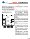
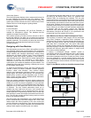
PRELIMINARY CY8CNP102B, CY8CNP102E
Document #: 001-43991 Rev. *D Page 11 of 38
DC Electrical Characteristics
The following DC electrical specifications list the guaranteed maximum and minimum specifications for the voltage and temperature
range: 3.0V to 3.6V over the Temperature range of -40°C ≤ T
A
≤ 85°C. Typical parameters apply to 3.3V at 25°C and are for design
guidance only.
DC Chip Level Specifications
DC General Purpose IO Specifications
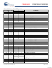
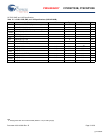
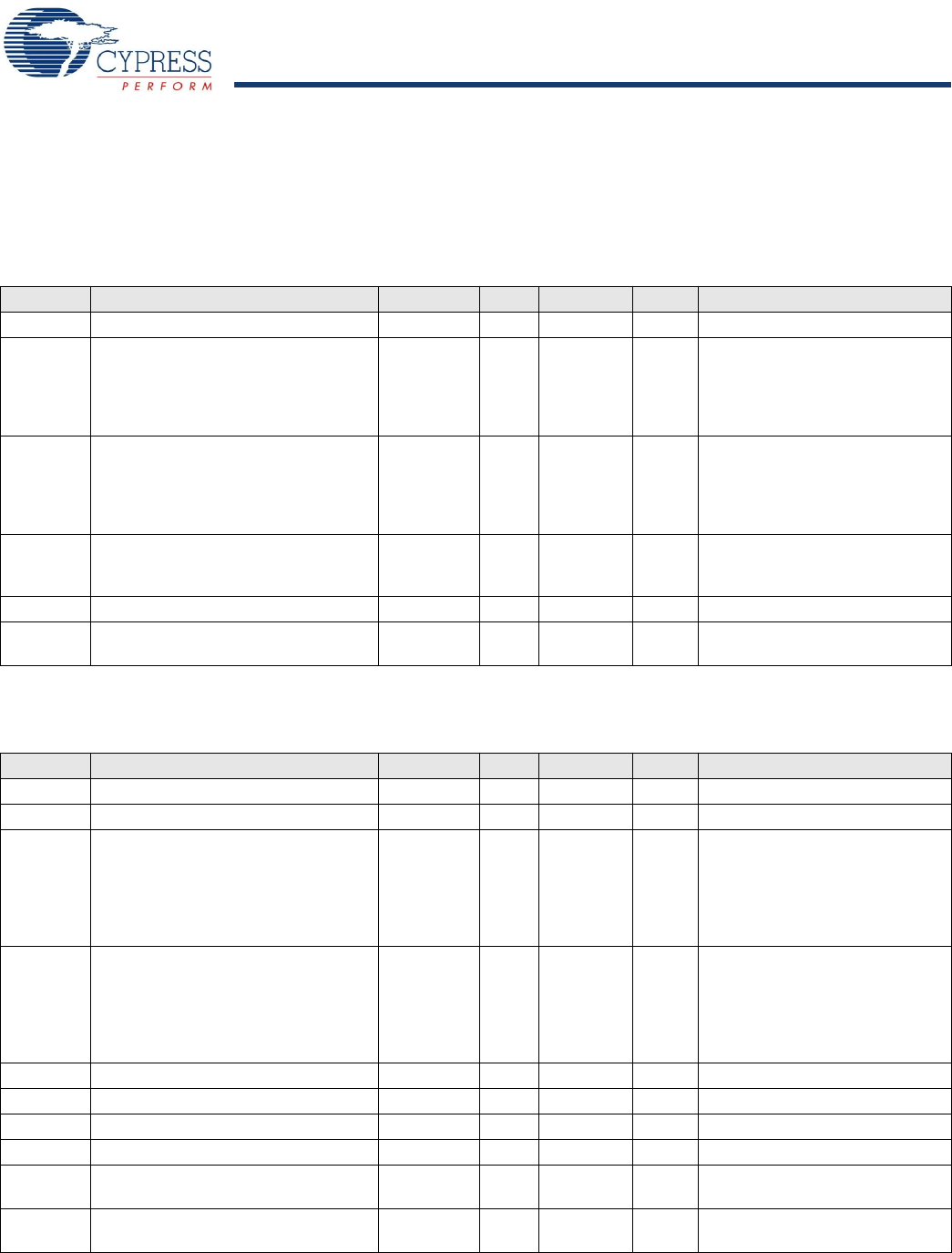
Table 5. 3.3V DC Chip Level Specifications (CY8CNP102B)
Symbol Description Min Typ Max Units Notes
Vcc Supply Voltage 3.00 – 3.6 V
I
DD
Supply Current – 36 40 mA T
A
= 25
o
C, CPU = 3 MHz,
SYSCLK doubler disabled,
VC1 = 1.5 MHz, VC2 = 93.75 kHz,
VC3 = 0.366 kHz, continuous
nvSRAM access
I
DDP
Supply current when IMO = 6 MHz
using SLIMO mode.
– 27 28 mA T
A
= 25
o
C, CPU = 0.75 MHz,
SYSCLK doubler disabled,
VC1=0.375 MHz, VC2=23.44 kHz,
VC3 = 0.09 kHz, continuous
nvSRAM access
I
SB
Sleep (Mode) Current with POR, LVD,
Sleep Timer, WDT, and internal slow
oscillator active.
– – 5 mA nvSRAM in standby.
V
REF
Reference Voltage (Bandgap) 1.28 1.3 1.32 V Trimmed for appropriate Vcc.
V
cap
Storage Capacitor between Vcap and
Vss
61 68 82 uF 5V rated (minimum)
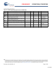
Table 6. 3.3V DC GPIO Specifications (CY8CNP102B)
Symbol Description Min Typ Max Units Notes
R
PU
Pull up Resistor 4 5.6 8 KΩ
R
PD
Pull down Resistor 4 5.6 8 KΩ
V
OH
High Output Level Vcc - 1.0 – – V IOH = 10 mA, Vcc = 3.0 to 3.6V. 8
total loads, 4 on even port pins (for
example, P0[2], P1[4]), 4 on odd
port pins (for example, P0[3],
P1[5]). 80 mA maximum combined
IOH budget.
V
OL
Low Output Level – – 0.75 V IOL = 25 mA, Vcc = 3.0 to 3.6V
8 total loads, 4 on even port pins
(for example, P0[2], P1[4]), 4 on
odd port pins (for example, P0[3],
P1[5]). 150 mA maximum
combined IOL budget.
V
IL
Input Low Level – – 0.8 V Vcc = 3.0 to 3.6
V
IH
Input High Level 1.6 – V Vcc = 3.0 to 3.6
V
H
Input Hysterisis – 60 – mV
I
IL
Input Leakage (Absolute Value) – 1 – nA Gross tested to 1 μA.
C
IN
Capacitive Load on Pins as Input – 3.5 10 pF Pin dependent.
Temp = 25
o
C.
C
OUT
Capacitive Load on Pins as Output – 3.5 10 pF Pin dependent.
Temp = 25
o
C.
[+] Feedback