


PRELIMINARY CY8CNP102B, CY8CNP102E
Document #: 001-43991 Rev. *D Page 31 of 38
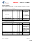
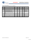
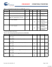
AC Analog Output Buffer Specifications
CRCPRS
(CRC Mode)
Maximum Input Clock Frequency – – 24.6 MHz 4.75V ≤ Vcc ≤ 5.25V.
SPIM Maximum Input Clock Frequency – – 8.2 MHz Maximum data rate at
4.1 MHz due to 2 x
over clocking.
SPIS Maximum Input Clock Frequency – – 4.1 ns
Width of SS_ Negated Between Transmis-
sions
50
[8]
– – ns
Transmitter Maximum Input Clock Frequency
Vcc ≥ 4.75V, 2 Stop Bits
– – 24.6 MHz Maximum data rate at
3.08 MHz due to 8 x
over clocking.
– – 49.2 MHz Maximum data rate at
6.15 MHz due to 8 x
over clocking.
Receiver Maximum Input Clock Frequency
Vcc ≥ 4.75V, 2 Stop Bits
– – 24.6 MHz Maximum data rate at
3.08 MHz due to 8 x
over clocking.
– – 49.2 MHz Maximum data rate at
6.15 MHz due to 8 x
over clocking.
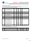
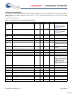
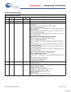
Table 38. 5V AC Analog Output Buffer Specifications (CY8CNP102E)
Symbol Description Min Typ Max Units
T
ROB
Rising Settling Time to 0.1%, 1V Step, 100 pF Load
Power = Low – – 4 μs
Power = High – – 4 μs
T
SOB
Falling Settling Time to 0.1%, 1V Step, 100 pF Load
Power = Low – – 3.4 μs
Power = High – – 3.4 μs
SR
ROB
Rising Slew Rate (20% to 80%), 1V Step, 100 pF Load
Power = Low 0.5 – – V/μs
Power = High 0.5 – – V/μs
SR
FOB
Falling Slew Rate (80% to 20%), 1V Step, 100 pF Load
Power = Low 0.55 – – V/μs
Power = High 0.55 – – V/μs
BW
OB
Small Signal Bandwidth, 20mV
pp
, 3dB BW, 100 pF Load
Power = Low 0.8 – – MHz
Power = High 0.8 – – MHz
BW
OB
Large Signal Bandwidth, 1V
pp
, 3dB BW, 100 pF Load
Power = Low 300 – – kHz
Power = High 300 – – kHz
Table 37. 5V AC Digital Block Specifications (CY8CNP102E) (continued)
Function Description Min Typ Max Units Notes
[+] Feedback